NCP1203GEVB ON Semiconductor, NCP1203GEVB Datasheet - Page 2
NCP1203GEVB
Manufacturer Part Number
NCP1203GEVB
Description
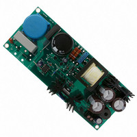
EVAL BOARD FOR NCP1203G
Manufacturer
ON Semiconductor
Specifications of NCP1203GEVB
Design Resources
NCP1203GEVB BOM NCP1203GEVB Gerber Files NCP1203 EVB Schematic
Main Purpose
AC/DC, Primary Side
Outputs And Type
1, Isolated
Voltage - Output
19V
Current - Output
4A
Voltage - Input
85 ~ 230VAC
Regulator Topology
Flyback
Frequency - Switching
60kHz
Board Type
Fully Populated
Utilized Ic / Part
NPC1200
Lead Free Status / RoHS Status
Lead free / RoHS Compliant
Power - Output
-
Lead Free Status / Rohs Status
Lead free / RoHS Compliant
For Use With/related Products
NCP1203G
Other names
NCP1203GEVBOS


Self-Powering the Controller in Standby
self-supply problem with a continuous pulses flow. In
standby, whatever implemented frequency reduction
techniques (e.g. skip or frequency foldback), the recurrence
between pulses can become very low. By definition, the
feedback loop manages to keep the energy content in each
burst high enough to maintain the nominal output voltage.
However, on the auxiliary side, it can be difficult to keep the
Vcc above the controller’s UVLO. Remember, to
permanently disable the DSS, you need to guarantee a level
above VccON max. which is 11 V for the NCP1200. Failure
to do this will re-activate the DSS in no-load conditions and
standby power will be degraded. Figure 1 offers a view of a
typical bunch of pulses captured in standby at a 127 VDC
input voltage.
16.5 V output level. The maximum rating for the NCP1200
states a level less than 16 V. As a result, the auxiliary Vcc
shall be less than 16V but also above VccON in any
conditions to ensure full DSS de-activation. A solution
consists in artificially raising the ratio between the power
winding and the auxiliary one to ensure adequate supply at
no-load. We successfully tested a 0.9 ratio, where the
An auxiliary winding does not usually cause any
As we previously stated, we want to deliver 70 W with a
1
2
3
4
Figure 1. A Bunch of Auxiliary Pulses Captured
NCP1200
Figure 2. The Auxiliary Is Clamped to Avoid
While the Supply Operates at No-Load
Exceeding the 16 V Maximum Rating
8
7
6
5
200 s
CVcc
(Vin = 127 VDC)
33 ms
3
15 V
Rlimit
2
Caux
1N4148
http://onsemi.com
1
Laux
AND8076/D
2
auxiliary output gets clamped by a 15V Zener diode in
nominal operation. Figure 2 shows the option.
90 VAC. Rlimit on Figure 2 can easily be adjusted to move
these values up or down, depending on the final winding
ratios. Care must be taken to avoid over-dissipation of the
15 V Zener diode in nominal conditions.
Power Supply, Element-by-Element Design
procedure for every component of the power supply.
DC High-Voltage Rail
high-voltage rail, neglecting the dual Vf drop:
Bulk Capacitor
bulk capacitor delivering power to a given charge. To
simplify the calculation, we will neglect the charging period
and thus consider a total discharge time equal to 1/(2 Fline).
From the design characteristics, we can evaluate the
equivalent current (Iload) drawn by the charge at the lowest
input line condition. Let’s us adopt a 40% ripple level, or a
50 V drop from the corresponding Vin
equivalent load current (which discharges Cbulk between
We measured a Vcc of 11.5 V @ 230 VAC and 12.2 V @
Let’s first detail the specs of our power supply:
Vin: 90–265 VAC
Vout: 16.8 V @ 4.2 A (Pout = 70 W)
Short-circuit protection
Over-voltage protection
Efficiency > 80%
Pin = 70 / 0.8 = 87.5
The below sequence details step-by-step the calculation
From these above numbers, we can deduce the level of the
Figure 3 portrays the typical waveform captured across a
Figure 3. A Typical Ripple Voltage Over the Bulk
Vripple
V HV max + 265 @ 2 + 374 VDC
V HV min + 90 @ 2 + 127 VDC
Capacitor
10 ms
Vinpeak
V
HV
avg
peak
. To evaluate the
Related parts for NCP1203GEVB
Image
Part Number
Description
Manufacturer
Datasheet
Request
R

Part Number:
Description:
Current Mode Controller Fixed Frequency Operation
Manufacturer:
ON Semiconductor
Datasheet:
Part Number:
Description:
ON Semiconductor [VOLTAGE REGULATOR]
Manufacturer:
ON Semiconductor
Datasheet:
Part Number:
Description:
357-036-542-201 CARDEDGE 36POS DL .156 BLK LOPRO
Manufacturer:
ON Semiconductor
Datasheet:
Part Number:
Description:
357-036-542-201 CARDEDGE 36POS DL .156 BLK LOPRO
Manufacturer:
ON Semiconductor
Datasheet:
Part Number:
Description:
357-036-542-201 CARDEDGE 36POS DL .156 BLK LOPRO
Manufacturer:
ON Semiconductor
Datasheet:
Part Number:
Description:
357-036-542-201 CARDEDGE 36POS DL .156 BLK LOPRO
Manufacturer:
ON Semiconductor
Datasheet:
Part Number:
Description:
357-036-542-201 CARDEDGE 36POS DL .156 BLK LOPRO
Manufacturer:
ON Semiconductor
Datasheet:
Part Number:
Description:
357-036-542-201 CARDEDGE 36POS DL .156 BLK LOPRO
Manufacturer:
ON Semiconductor
Datasheet:
Part Number:
Description:
357-036-542-201 CARDEDGE 36POS DL .156 BLK LOPRO
Manufacturer:
ON Semiconductor
Datasheet:
Part Number:
Description:
357-036-542-201 CARDEDGE 36POS DL .156 BLK LOPRO
Manufacturer:
ON Semiconductor
Datasheet:
Part Number:
Description:
357-036-542-201 CARDEDGE 36POS DL .156 BLK LOPRO
Manufacturer:
ON Semiconductor
Datasheet:
Part Number:
Description:
357-036-542-201 CARDEDGE 36POS DL .156 BLK LOPRO
Manufacturer:
ON Semiconductor
Datasheet:
Part Number:
Description:
Manufacturer:
ON Semiconductor
Datasheet:
Part Number:
Description:
Manufacturer:
ON Semiconductor
Datasheet: