NCP1203GEVB ON Semiconductor, NCP1203GEVB Datasheet - Page 8
NCP1203GEVB
Manufacturer Part Number
NCP1203GEVB
Description
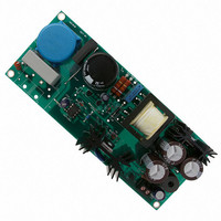
EVAL BOARD FOR NCP1203G
Manufacturer
ON Semiconductor
Specifications of NCP1203GEVB
Design Resources
NCP1203GEVB BOM NCP1203GEVB Gerber Files NCP1203 EVB Schematic
Main Purpose
AC/DC, Primary Side
Outputs And Type
1, Isolated
Voltage - Output
19V
Current - Output
4A
Voltage - Input
85 ~ 230VAC
Regulator Topology
Flyback
Frequency - Switching
60kHz
Board Type
Fully Populated
Utilized Ic / Part
NPC1200
Lead Free Status / RoHS Status
Lead free / RoHS Compliant
Power - Output
-
Lead Free Status / Rohs Status
Lead free / RoHS Compliant
For Use With/related Products
NCP1203G
Other names
NCP1203GEVBOS


Transformer
transformer manufacturer to help him select the right
winding size and tailor the internal gap:
propagation delay: 1 / 0.33 + 374
Clamping Network
following formulae:
P Rclamp + 1
with:
clamping level of 150 V, Rclamp is found to be 4.7 k /6 W
and Cclamp 100 nF. The RMS current flowing through
Cclamp is 220 mA. RC networks are economical clamping
devices and care must be taken to not exceed the MOSFET
BVdss in the most stringent conditions, e.g. a cold startup
sequence at high line. Worse case arises when Ip is
maximum and Vout reaches the target.
Stability Analysis
approaches. Spice has proven to be rather accurate for
feedback loop analysis with SMPS. We will use the
NCP1200 average model which is available to download
from our web site (www.onsemi.com/pub/ncp1200). Figure
10 shows the simulation template where the feedback
network on the TL431 has been simplified to a simple 100nF
capacitor.
short and results are delivered in a snap-shot, as testified by
Figure 11. Figure 12 unveils the results obtained using a
Rclamp
Below are the key parameters you will pass to your
Maximum peak primary current, including 160 ns
Maximum primary RMS current at low line: 1.6 A
Maximum secondary RMS current: 6.9 A
Primary inductance: 700 H
Turn-ratio, power section: Np:Ns = 1:0.166
Turn-ratio, auxiliary section: Np:Naux = 1:0.15
The clamping network can be calculated using the
The power dissipated by Rclamp can also be expressed by:
Vclamp: the desired clamping level;
Ip: the maximum peak current (e.g. during overload);
Vout + Vf: the regulated output voltage level + the
Lleak: the primary leakage inductance;
N: the Ns:Np conversion ratio;
Fsw: the switching frequency;
Vripple: the clamping ripple, could be around 20 V.
With a measured leakage inductance of 12 H and a final
The stability analysis can be investigated using different
Thanks to average modeling, the simulation time is kept
secondary diode voltage drop;
+
2 @ Vclamp @ (Vclamp * (Vout ) Vf sec) @ N)
Cclamp +
2
@ Lleak @ Ip 2 @ F SW @
Lleak @ Ip 2 @ F SW
Vripple @ F SW @ Rclamp
Vclamp
160 n / 700
(Vout)Vf sec)@N
(Vout)Vf sec)@N
Vclamp
Vclamp
* 1
= 3.2 A
http://onsemi.com
AND8076/D
(22)
(23)
(24)
8
network analyzer and confirms the validity of our approach
(Vin = 240 VAC).
combinations and gave good results. Final transient step did
not reveal any overshoot or unwanted oscillations.
The Adapter Schematic
architecture, driving a 600 V MOSFET. The 2SK2545
features a 10 A capability but a 6.0 A/600 V can also be
mounted, such as the FQP6N60 from Fairchild but to the
expense of increased conduction losses. Figure 13 offers a
complete view of the electrical sketch. The board can
actually be used with either auxiliary or without auxiliary
winding. By removing the resistance R4, you reactivate the
DSS on a NCP120X controller featuring this ability. The
board can therefore accept the following controllers:
NCP1200, featuring DSS.
NCP1200A, featuring DSS.
NCP1203, auxiliary winding only.
NCP1216, featuring DSS and internal ramp compensation.
Improved EMI jittering with DSS.
NCP1217,
compensation.
avoids using the external circuitry made of R1-R7-D4 and
C10. If one of these two parts are plugged in the demoboard,
you must disable this network by simply disconnecting R1
and growing R6 up to 2.7 k (for a 65 kHz operation).
implement a discrete SCR, activated in presence of an OVP,
e.g. an optocoupler failure. D5 senses the overvoltage
condition and can easily be adjusted to fit any other levels.
Thanks to R10, the OVP permanently latches-off the supply
and the user shall cycle V
supply. Shutdown is obtained by pulling the feedback pin
down through D6. The clamp resistor is split in two different
components to avoid an excessive heat burden on one single
device. Both main MOSFET and secondary diode are
mounted on an adequate heatsink to evacuate the heat.
board performance faster, we have experimented different
transformers, available through Appendix B manufacturers.
Please note that some include the auxiliary winding for DSS
deactivation whereas other only offer a dual winding
arrangement where the DSS no longer activates and offers
the best standby power. All details are given in appendix B.
The final demoboard will not accommodate with all these
transformers simply because multiple footprints was not
possible. They however have all been tested okay.
Measurements were taken with the Coilcraft transformer.
19 VDC/70 W versus the original design-based 16.5 V. As
a result, figure 1b circuit has been replaced by L3-R13 and
C12 to improve the short-circuit protection when using an
auxiliary winding. Output voltage can be adjusted by
changing the feedback network made of R12/R20/R21.
Stability has been checked at various line/loads
The final schematic implements a current-mode Flyback
On NCP1216 and 1217, the internal ramp compensation
The NCP120X takes place with two other bipolars that
To ease the designer task, or simply help evaluating the
As a final note, the actual demoboard delivers
auxiliary
winding
CC
off and on again to restart the
only,
internal
ramp
Related parts for NCP1203GEVB
Image
Part Number
Description
Manufacturer
Datasheet
Request
R

Part Number:
Description:
Current Mode Controller Fixed Frequency Operation
Manufacturer:
ON Semiconductor
Datasheet:
Part Number:
Description:
ON Semiconductor [VOLTAGE REGULATOR]
Manufacturer:
ON Semiconductor
Datasheet:
Part Number:
Description:
357-036-542-201 CARDEDGE 36POS DL .156 BLK LOPRO
Manufacturer:
ON Semiconductor
Datasheet:
Part Number:
Description:
357-036-542-201 CARDEDGE 36POS DL .156 BLK LOPRO
Manufacturer:
ON Semiconductor
Datasheet:
Part Number:
Description:
357-036-542-201 CARDEDGE 36POS DL .156 BLK LOPRO
Manufacturer:
ON Semiconductor
Datasheet:
Part Number:
Description:
357-036-542-201 CARDEDGE 36POS DL .156 BLK LOPRO
Manufacturer:
ON Semiconductor
Datasheet:
Part Number:
Description:
357-036-542-201 CARDEDGE 36POS DL .156 BLK LOPRO
Manufacturer:
ON Semiconductor
Datasheet:
Part Number:
Description:
357-036-542-201 CARDEDGE 36POS DL .156 BLK LOPRO
Manufacturer:
ON Semiconductor
Datasheet:
Part Number:
Description:
357-036-542-201 CARDEDGE 36POS DL .156 BLK LOPRO
Manufacturer:
ON Semiconductor
Datasheet:
Part Number:
Description:
357-036-542-201 CARDEDGE 36POS DL .156 BLK LOPRO
Manufacturer:
ON Semiconductor
Datasheet:
Part Number:
Description:
357-036-542-201 CARDEDGE 36POS DL .156 BLK LOPRO
Manufacturer:
ON Semiconductor
Datasheet:
Part Number:
Description:
357-036-542-201 CARDEDGE 36POS DL .156 BLK LOPRO
Manufacturer:
ON Semiconductor
Datasheet:
Part Number:
Description:
Manufacturer:
ON Semiconductor
Datasheet:
Part Number:
Description:
Manufacturer:
ON Semiconductor
Datasheet: