CDB4365 Cirrus Logic Inc, CDB4365 Datasheet - Page 29
CDB4365
Manufacturer Part Number
CDB4365
Description
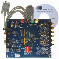
EVALUATION BOARD FOR CS4365
Manufacturer
Cirrus Logic Inc
Specifications of CDB4365
Number Of Dac's
6
Number Of Bits
24
Outputs And Type
6, Differential
Sampling Rate (per Second)
192k
Data Interface
Serial
Dac Type
Voltage
Voltage Supply Source
Analog and Digital
Operating Temperature
-40°C ~ 85°C
Utilized Ic / Part
CS4365
Description/function
Audio D/A
Operating Supply Voltage
5 V
Product
Audio Modules
For Use With/related Products
CS4365
Lead Free Status / RoHS Status
Contains lead / RoHS non-compliant
Lead Free Status / RoHS Status
Lead free / RoHS Compliant, Contains lead / RoHS non-compliant
Other names
598-1779


DS670F2
4.11
4.12
4.12.1 Hardware Mode
The MUTEC Outputs
The MUTEC1-6 pins have an auto-polarity detect feature. The MUTEC output pins are high impedance at
the time of reset. The external mute circuitry needs to be self-biased into an active state in order to be muted
during reset. Upon release of reset, the CS4365 will detect the status of the MUTEC pins (high or low) and
will then select that state as the polarity to drive when the mutes become active. The external-bias voltage
level that the MUTEC pins see at the time of release of reset must meet the “MUTEC auto-detect input
high/low voltage” specifications as outlined in the Digital Characteristics section.
Figure 21
signs, the pull-up and pull-down resistors have been especially chosen to meet the input high/low threshold
when used with the MMUN2111 and MMUN2211 internal bias resistances of 10 kΩ. Use of the Mute Control
function is not mandatory, but recommended, for designs requiring the absolute minimum in extraneous
clicks and pops. Also, use of the Mute Control function can enable the system designer to achieve idle chan-
nel noise/signal-to-noise ratios which are only limited by the external mute circuit.
Recommended Power-Up Sequence
1. Hold RST low until the power supplies and configuration pins are stable, and the master and left/right
2. Bring RST high. The device will remain in a low power state with FILT+ low and will initiate the
clocks are locked to the appropriate frequencies, as discussed in
registers are reset to the default settings, FILT+ will remain low, and VQ will be connected to VA/2.
If RST can not be held low long enough the SDINx pins should remain static low until all other clocks
are stable, and if possible the RST should be toggled low again once the system is stable.
Hardware power-up sequence after approximately 512 LRCK cycles in Single-Speed Mode (1024
LRCK cycles in Double-Speed Mode, and 2048 LRCK cycles in Quad-Speed Mode).
shows a single example of both an active high and an active low mute drive circuit. In these de-
Figure 21. Recommended Mute Circuitry
Section
4.1. In this state, the
CS4365
29
Related parts for CDB4365
Image
Part Number
Description
Manufacturer
Datasheet
Request
R

Part Number:
Description:
Development Kit
Manufacturer:
Cirrus Logic Inc
Datasheet:
Part Number:
Description:
Development Kit
Manufacturer:
Cirrus Logic Inc
Datasheet:


Part Number:
Description:
High-efficiency PFC + Fluorescent Lamp Driver Reference Design
Manufacturer:
Cirrus Logic Inc
Datasheet:
Part Number:
Description:
Development Kit
Manufacturer:
Cirrus Logic Inc
Datasheet:
Part Number:
Description:
Development Kit
Manufacturer:
Cirrus Logic Inc
Datasheet:

Part Number:
Description:
Development Kit
Manufacturer:
Cirrus Logic Inc
Datasheet:
Part Number:
Description:
Development Kit
Manufacturer:
Cirrus Logic Inc
Datasheet:
Part Number:
Description:
Development Kit
Manufacturer:
Cirrus Logic Inc
Datasheet:
Part Number:
Description:
Development Kit
Manufacturer:
Cirrus Logic Inc
Datasheet:

Part Number:
Description:
EVALUATION BOARD FOR CS8427
Manufacturer:
Cirrus Logic Inc
Datasheet:

Part Number:
Description:
BOARD EVAL FOR CS8416 RCVR
Manufacturer:
Cirrus Logic Inc
Datasheet:

Part Number:
Description:
EVALUATION BOARD FOR CS8420
Manufacturer:
Cirrus Logic Inc
Datasheet:

Part Number:
Description:
KIT DEVELOPMENT EP9315 ARM9
Manufacturer:
Cirrus Logic Inc
Datasheet:

Part Number:
Description:
KIT DEVELOPMENT EP9302 ARM9
Manufacturer:
Cirrus Logic Inc
Datasheet: