CDB4365 Cirrus Logic Inc, CDB4365 Datasheet - Page 31
CDB4365
Manufacturer Part Number
CDB4365
Description
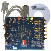
EVALUATION BOARD FOR CS4365
Manufacturer
Cirrus Logic Inc
Specifications of CDB4365
Number Of Dac's
6
Number Of Bits
24
Outputs And Type
6, Differential
Sampling Rate (per Second)
192k
Data Interface
Serial
Dac Type
Voltage
Voltage Supply Source
Analog and Digital
Operating Temperature
-40°C ~ 85°C
Utilized Ic / Part
CS4365
Description/function
Audio D/A
Operating Supply Voltage
5 V
Product
Audio Modules
For Use With/related Products
CS4365
Lead Free Status / RoHS Status
Contains lead / RoHS non-compliant
Lead Free Status / RoHS Status
Lead free / RoHS Compliant, Contains lead / RoHS non-compliant
Other names
598-1779


DS670F2
4.14.2.1 I²C Write
To write to the device, follow the procedure below while adhering to the control port Switching Specifica-
tions in
1. Initiate a START condition to the I²C bus followed by the address byte. The upper 6 bits must be
2. Wait for an acknowledge (ACK) from the part, then write to the memory address pointer, MAP. This
3. Wait for an acknowledge (ACK) from the part, then write the desired data to the register pointed to by
4. If the INCR bit (see
5. If the INCR bit is set to 0 and further I²C writes to other registers are desired, it is necessary to initiate
4.14.2.2 I²C Read
To read from the device, follow the procedure below while adhering to the control port Switching Specifi-
cations.
1. Initiate a START condition to the I²C bus followed by the address byte. The upper 6 bits must be
2. After transmitting an acknowledge (ACK), the device will then transmit the contents of the register
3. Once the device has transmitted the contents of the register pointed to by the MAP, issue an ACK.
4. If the INCR bit is set to 1, the device will continue to transmit the contents of successive registers. Con-
5. If the INCR bit is set to 0 and further I²C reads from other registers are desired, it is necessary to initiate
001100. The seventh bit must match the setting of the AD0 pin, and the eighth must be 0. The eighth
bit of the address byte is the R/W bit.
byte points to the register to be written.
the MAP.
are written, then initiate a STOP condition to the bus.
a repeated START condition and follow the procedure detailed from step 1. If no further writes to other
registers are desired, initiate a STOP condition to the bus.
001100. The seventh bit must match the setting of the AD0 pin, and the eighth must be 1. The eighth
bit of the address byte is the R/W bit.
pointed to by the MAP. The MAP register will contain the address of the last register written to the
MAP, or the default address (see
device.
tinue providing a clock and issue an ACK after each byte until all the desired registers are read, then
initiate a STOP condition to the bus.
a repeated START condition and follow the procedure detailed from steps 1 and 2 from the I²C Write
instructions followed by step 1 of the I²C Read section. If no further reads from other registers are de-
sired, initiate a STOP condition to the bus.
Section
S D A
S C L
N ote: If operation is a w rite, th is byte contain s the M em o ry A ddress P ointer, M A P.
Start
.
001100
Section
Figure 22. Control Port Timing, I²C Mode
ADDR
AD 0
4.14.1) is set to 1, repeat the previous step until all the desired registers
Section
R/W
ACK
4.14.1) if an I²C read is the first operation performed on the
DATA
1-8
N ote 1
ACK
DATA
1-8
ACK
Stop
CS4365
31
Related parts for CDB4365
Image
Part Number
Description
Manufacturer
Datasheet
Request
R

Part Number:
Description:
Development Kit
Manufacturer:
Cirrus Logic Inc
Datasheet:
Part Number:
Description:
Development Kit
Manufacturer:
Cirrus Logic Inc
Datasheet:


Part Number:
Description:
High-efficiency PFC + Fluorescent Lamp Driver Reference Design
Manufacturer:
Cirrus Logic Inc
Datasheet:
Part Number:
Description:
Development Kit
Manufacturer:
Cirrus Logic Inc
Datasheet:
Part Number:
Description:
Development Kit
Manufacturer:
Cirrus Logic Inc
Datasheet:

Part Number:
Description:
Development Kit
Manufacturer:
Cirrus Logic Inc
Datasheet:
Part Number:
Description:
Development Kit
Manufacturer:
Cirrus Logic Inc
Datasheet:
Part Number:
Description:
Development Kit
Manufacturer:
Cirrus Logic Inc
Datasheet:
Part Number:
Description:
Development Kit
Manufacturer:
Cirrus Logic Inc
Datasheet:

Part Number:
Description:
EVALUATION BOARD FOR CS8427
Manufacturer:
Cirrus Logic Inc
Datasheet:

Part Number:
Description:
BOARD EVAL FOR CS8416 RCVR
Manufacturer:
Cirrus Logic Inc
Datasheet:

Part Number:
Description:
EVALUATION BOARD FOR CS8420
Manufacturer:
Cirrus Logic Inc
Datasheet:

Part Number:
Description:
KIT DEVELOPMENT EP9315 ARM9
Manufacturer:
Cirrus Logic Inc
Datasheet:

Part Number:
Description:
KIT DEVELOPMENT EP9302 ARM9
Manufacturer:
Cirrus Logic Inc
Datasheet: