CDB4365 Cirrus Logic Inc, CDB4365 Datasheet - Page 38
CDB4365
Manufacturer Part Number
CDB4365
Description
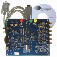
EVALUATION BOARD FOR CS4365
Manufacturer
Cirrus Logic Inc
Specifications of CDB4365
Number Of Dac's
6
Number Of Bits
24
Outputs And Type
6, Differential
Sampling Rate (per Second)
192k
Data Interface
Serial
Dac Type
Voltage
Voltage Supply Source
Analog and Digital
Operating Temperature
-40°C ~ 85°C
Utilized Ic / Part
CS4365
Description/function
Audio D/A
Operating Supply Voltage
5 V
Product
Audio Modules
For Use With/related Products
CS4365
Lead Free Status / RoHS Status
Contains lead / RoHS non-compliant
Lead Free Status / RoHS Status
Lead free / RoHS Compliant, Contains lead / RoHS non-compliant
Other names
598-1779


38
6.5
6.5.1 Interpolation Filter Select (FILT_SEL)
6.6
6.6.1 Invert Signal Polarity (Inv_xx)
6.7
6.7.1 Mute Pin Control (MUTEC1, MUTEC0)
Reserved
Reserved
MUTEC1
0
0
0
7
7
7
Filter Control (address 05h)
Invert Control (address 06h)
Group Control (address 07h)
Function:
When set to 0 (default), the Interpolation Filter has a fast roll-off.
When set to 1, the Interpolation Filter has a slow roll-off.
The specifications for each filter can be found in the Analog characteristics table, and response plots can
be found in
Function:
When set to 1, this bit inverts the signal polarity of channel xx.
When set to 0 (default), this function is disabled.
Default = 00
00 - Six mute control signals
01, 10 - One mute control signal
11 - Three mute control signals
Function:
Selects how the internal mute control signals are routed to the MUTEC1 through MUTEC6 pins. When
set to ‘00’, there is one mute control signal for each channel: AOUT1A on MUTEC1, AOUT1B on
MUTEC2, etc. When set to ‘01’ or ‘10’, there is a single mute control signal on the MUTEC1 pin. When
set to ‘11’, there are three mute control signals, one for each stereo pair: AOUT1A and AOUT1B on
MUTEC1, AOUT2A and AOUT2B on MUTEC2, and AOUT3A and AOUT3B on MUTEC3.
Reserved
Reserved
MUTEC0
6
0
6
0
6
0
Figures 24
Reserved
Reserved
INV_B3
to 47.
5
0
5
0
5
0
Reserved
P1_A=B
INV_A3
0
0
0
4
4
4
Reserved
P2_A=B
INV_B2
3
0
3
0
3
0
Reserved
P3_A=B
INV_A2
2
0
2
0
2
0
Reserved
Reserved
INV_B1
0
0
0
1
1
1
SNGLVOL
FILT_SEL
CS4365
INV_A1
DS670F2
0
0
0
0
0
0
Related parts for CDB4365
Image
Part Number
Description
Manufacturer
Datasheet
Request
R

Part Number:
Description:
Development Kit
Manufacturer:
Cirrus Logic Inc
Datasheet:
Part Number:
Description:
Development Kit
Manufacturer:
Cirrus Logic Inc
Datasheet:


Part Number:
Description:
High-efficiency PFC + Fluorescent Lamp Driver Reference Design
Manufacturer:
Cirrus Logic Inc
Datasheet:
Part Number:
Description:
Development Kit
Manufacturer:
Cirrus Logic Inc
Datasheet:
Part Number:
Description:
Development Kit
Manufacturer:
Cirrus Logic Inc
Datasheet:

Part Number:
Description:
Development Kit
Manufacturer:
Cirrus Logic Inc
Datasheet:
Part Number:
Description:
Development Kit
Manufacturer:
Cirrus Logic Inc
Datasheet:
Part Number:
Description:
Development Kit
Manufacturer:
Cirrus Logic Inc
Datasheet:
Part Number:
Description:
Development Kit
Manufacturer:
Cirrus Logic Inc
Datasheet:

Part Number:
Description:
EVALUATION BOARD FOR CS8427
Manufacturer:
Cirrus Logic Inc
Datasheet:

Part Number:
Description:
BOARD EVAL FOR CS8416 RCVR
Manufacturer:
Cirrus Logic Inc
Datasheet:

Part Number:
Description:
EVALUATION BOARD FOR CS8420
Manufacturer:
Cirrus Logic Inc
Datasheet:

Part Number:
Description:
KIT DEVELOPMENT EP9315 ARM9
Manufacturer:
Cirrus Logic Inc
Datasheet:

Part Number:
Description:
KIT DEVELOPMENT EP9302 ARM9
Manufacturer:
Cirrus Logic Inc
Datasheet: