CDB4365 Cirrus Logic Inc, CDB4365 Datasheet - Page 7
CDB4365
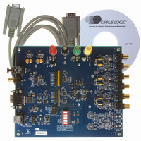
Manufacturer Part Number
CDB4365
Description
EVALUATION BOARD FOR CS4365
Manufacturer
Cirrus Logic Inc
Specifications of CDB4365
Number Of Dac's
6
Number Of Bits
24
Outputs And Type
6, Differential
Sampling Rate (per Second)
192k
Data Interface
Serial
Dac Type
Voltage
Voltage Supply Source
Analog and Digital
Operating Temperature
-40°C ~ 85°C
Utilized Ic / Part
CS4365
Description/function
Audio D/A
Operating Supply Voltage
5 V
Product
Audio Modules
For Use With/related Products
CS4365
Lead Free Status / RoHS Status
Contains lead / RoHS non-compliant
Lead Free Status / RoHS Status
Lead free / RoHS Compliant, Contains lead / RoHS non-compliant
Other names
598-1779


DS670F2
VQ
FILT+
AOUTA1 +,-
AOUTB1 +,-
AOUTA2 +,-
AOUTB2 +,-
AOUTA3 +,-
AOUTB3 +,-
MUTEC1
MUTEC2
MUTEC3
MUTEC4
MUTEC5
MUTEC6
Hardware Mode Definitions
M0
M1
M2
M3
M4
Software Mode Definitions
SCL/CCLK
SDA/CDIN
AD0/CS
TST
DSD Definitions
DSDA1
DSDB1
DSDA2
DSDB2
DSDA3
DSDB3
DSD_SCLK
Pin Name
10, 12
39,40
37,38
35,36
33,34
29,30
27,28
21
20
41
26
25
24
23
22
17
16
15
12
10
15
16
17
48
47
46
42
#
3
2
1
Quiescent Voltage (Output) - Filter connection for internal quiescent voltage. VQ must be
capacitively coupled to analog ground, as shown in the Typical Connection Diagram. The nom-
inal voltage level is specified in the Analog Characteristics and Specifications section. VQ pre-
sents an appreciable source impedance and any current drawn from this pin will alter device
performance. However, VQ can be used to bias the analog circuitry assuming there is no AC
signal component and the DC current is less then the maximum specified in the Analog Char-
acteristics and Specifications section.
Positive Voltage Reference (Output) - Positive reference voltage for the internal sampling cir-
cuits. Requires the capacitive decoupling to analog ground as shown in the Typical Connection
Diagram.
Differential Analog Output (Output) - The full-scale differential analog output level is specified
in the Analog Characteristics specification table.
Mute Control (Output) - The Mute Control pins go high during power-up initialization, reset,
muting, power-down or if the master clock to left/right clock frequency ratio is incorrect. These
pins are intended to be used as a control for external mute circuits on the line outputs to pre-
vent the clicks and pops that can occur in any single supply system. Use of Mute Control is not
mandatory but recommended for designs requiring the absolute minimum in extraneous clicks
and pops.
Mode Selection (Input) - Determines the operational mode of the device as detailed in
and
Serial Control Port Clock (Input) - Serial clock for the serial control port. Requires an external
pull-up resistor to the logic interface voltage in I²C
Diagram.
Serial Control Port Data (Input/Output) - SDA is a data I/O line in I²C Mode and is open drain,
requiring an external pull-up resistor to the logic interface voltage, as shown in the Typical Con-
nection Diagram; CDIN is the input data line for the control port interface in SPI
Address Bit 0 (I²C) / Control Port Chip Select (SPI) (Input) - AD0 is a chip address pin in I²C
Mode; CS is the chip-select signal for SPI Mode.
Test - These pins need to be tied to analog ground.
Direct Stream Digital Input (Input) - Input for Direct Stream Digital serial audio data. GND if
unused.
DSD Serial Clock (Input) - Serial clock for the Direct Stream Digital serial audio interface.
Table
7.
Pin Description
®
Mode as shown in the Typical Connection
™
Mode.
CS4365
Table 6
7
Related parts for CDB4365
Image
Part Number
Description
Manufacturer
Datasheet
Request
R

Part Number:
Description:
Development Kit
Manufacturer:
Cirrus Logic Inc
Datasheet:
Part Number:
Description:
Development Kit
Manufacturer:
Cirrus Logic Inc
Datasheet:


Part Number:
Description:
High-efficiency PFC + Fluorescent Lamp Driver Reference Design
Manufacturer:
Cirrus Logic Inc
Datasheet:
Part Number:
Description:
Development Kit
Manufacturer:
Cirrus Logic Inc
Datasheet:
Part Number:
Description:
Development Kit
Manufacturer:
Cirrus Logic Inc
Datasheet:

Part Number:
Description:
Development Kit
Manufacturer:
Cirrus Logic Inc
Datasheet:
Part Number:
Description:
Development Kit
Manufacturer:
Cirrus Logic Inc
Datasheet:
Part Number:
Description:
Development Kit
Manufacturer:
Cirrus Logic Inc
Datasheet:
Part Number:
Description:
Development Kit
Manufacturer:
Cirrus Logic Inc
Datasheet:

Part Number:
Description:
EVALUATION BOARD FOR CS8427
Manufacturer:
Cirrus Logic Inc
Datasheet:

Part Number:
Description:
BOARD EVAL FOR CS8416 RCVR
Manufacturer:
Cirrus Logic Inc
Datasheet:

Part Number:
Description:
EVALUATION BOARD FOR CS8420
Manufacturer:
Cirrus Logic Inc
Datasheet:

Part Number:
Description:
KIT DEVELOPMENT EP9315 ARM9
Manufacturer:
Cirrus Logic Inc
Datasheet:

Part Number:
Description:
KIT DEVELOPMENT EP9302 ARM9
Manufacturer:
Cirrus Logic Inc
Datasheet: