EVAL-AD5425EBZ Analog Devices Inc, EVAL-AD5425EBZ Datasheet
EVAL-AD5425EBZ
Specifications of EVAL-AD5425EBZ


Related parts for EVAL-AD5425EBZ


EVAL-AD5425EBZ Summary of contents
Page 1
FEATURES 2 5.5 V supply operation 50 MHz serial interface 9.5 MSPS update rate INL of ±0.25 LSB 10 MHz multiplying bandwidth ±10 V reference input Low glitch energy: <2 nV-s Extended temperature range: −40°C to +125°C 10-lead ...
Page 2
... Change to Table 7 ..........................................................................18 2/04—Revision 0: Initial Version Adding Gain................................................................................ 17 DACs Used as a Divider or Programmable Gain Element ... 17 Reference Selection .................................................................... 17 Amplifier Selection .................................................................... 18 Serial Interface ............................................................................ 19 Microprocessor Interfacing....................................................... 19 PCB Layout and Power Supply Decoupling................................ 22 Evaluation Board ........................................................................ 22 Operating the Evaluation Board .............................................. 22 Outline Dimensions ....................................................................... 27 Ordering Guide .......................................................................... 27 Rev Page ...
Page 3
SPECIFICATIONS Temperature range for Y version: −40°C to +125°C. All specifications T DD REF OUT otherwise noted. DC performance measured with OP177, ac performance ...
Page 4
AD5425 Parameter Digital THD 50 kHz f OUT 20 kHz f OUT Output Noise Spectral Density SFDR Performance (Wide Band) 50 kHz f OUT 20 kHz f OUT SFDR Performance (Narrow Band) 50 kHz f OUT 20 kHz f OUT ...
Page 5
TIMING CHARACTERISTICS All input signals are specified with (10 temperature range for Y version: −40°C to +125°C ; all specifications T ...
Page 6
AD5425 ABSOLUTE MAXIMUM RATINGS T = 25°C, unless otherwise noted. A Table 3. Parameter Rating V to GND −0 GND − +12 V REF ...
Page 7
PIN CONFIGURATION AND FUNCTION DESCRIPTIONS Table 4. Pin Function Descriptions Pin No. Mnemonic Function DAC Current Output. OUT DAC Analog Ground. This pin should normally be tied to the analog ground of the system. ...
Page 8
AD5425 TYPICAL PERFORMANCE CHARACTERISTICS 0. 25° 10V REF 0. 0.10 0.05 0 –0.05 –0.10 –0.15 –0. 100 150 CODE Figure 4. INL vs. Code (8-Bit DAC) 0. ...
Page 9
T = 25° REF 0.3 MAX INL MAX DNL 0.1 –0.1 MIN DNL MIN INL –0.3 –0.5 0.5 0.6 0.7 0.8 0.9 1.0 1.1 1.2 V (V) BIAS Figure 10. Linearity ...
Page 10
AD5425 0 25°C A 0.6 0 0.4 0.3 0 2. INPUT VOLTAGE (V) Figure 16. Supply Current vs. Input Voltage 1.8 ...
Page 11
T = 25° 3.5V p-p REF –65 –70 –75 –80 –85 – 100 1k 10k FREQUENCY (Hz) Figure 22. THD and Noise vs. Frequency AMPLIFIER ...
Page 12
AD5425 0 –10 –20 –30 –40 –50 –60 –70 –80 –90 –100 10k 15k 20k 25k FREQUENCY (Hz) Figure 28. Narrowband IMD (±50%) Clock = 2 MHz kHz kHz OUT OUT V ...
Page 13
TERMINOLOGY Relative Accuracy Relative accuracy or endpoint nonlinearity is a measure of the maximum deviation from a straight line passing through the endpoints of the DAC transfer function measured after adjusting for zero and full scale and is ...
Page 14
AD5425 THEORY OF OPERATION The AD5425 is an 8-bit current output DAC consisting of a standard inverting R-2R ladder configuration. A simplified diagram is shown in Figure 29. The feedback resistor, R value of R. The value ...
Page 15
V REF R1 ±10V NOTES AND R2 ARE USED ONLY IF GAIN ADJUSTMENT IS REQUIRED. ADJUST R1 FOR V OUT 2. MATCHING AND TRACKING IS ESSENTIAL FOR RESISTOR PAIRS R3 AND R4 PHASE COMPENSATION (1pF TO ...
Page 16
AD5425 SINGLE-SUPPLY APPLICATIONS Current Mode Operation In the current mode circuit of Figure 32 biased positive by an amount applied to V configuration, the output voltage is given × × (V ...
Page 17
ADDING GAIN In applications where the output voltage is required to be greater than V , gain can be added with an additional external IN amplifier or it can be achieved in a single stage important to take ...
Page 18
AD5425 AMPLIFIER SELECTION The primary requirement for the current-steering mode is an amplifier with low input bias currents and low input offset vol- tage. The input offset voltage amp is multiplied by the variable gain (due to ...
Page 19
SERIAL INTERFACE The AD5425 has a simple 3-wire interface that is compatible with SPI, QSPI, MICROWIRE, and DSP interface standards. Data is written to the device in 8-bit words. This 8-bit word consists of 8 data bits, as shown in ...
Page 20
AD5425 ADSP-BF5xx-to-AD5425 Interface The ADSP-BF5xx family of processors has an SPI-compatible port that enables the processor to communicate with SPI- compatible devices. A serial interface between the ADSP-BF5xx and the AD5425 DAC is shown in Figure 40. In this configura- ...
Page 21
MICROWIRE-to-AD5425 Interface Figure 44 shows an interface between the DAC and any ™ MICROWIRE -compatible device. Serial data is shifted out on the falling edge of the serial clock, SK, and is clocked into the DAC input shift register on ...
Page 22
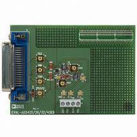
... I-to-V amplifier should be located as close to the device as possible. EVALUATION BOARD The board consists of an 8-bit AD5425 and a current-to-voltage amplifier, the AD8065. Included on the evaluation board reference, the ADR01. An external reference can also be applied via an SMB input. The evaluation kit consists of a CD-ROM with self-installing PC software to control the DAC ...
Page 23
... V P1–29 DD P1–30 P2–3 + C11 C12 0.1μF 10μF P2–2 AGND + C13 C14 0.1μF 10μF P2–1 V DD1 V SS P2–4 + C15 C16 0.1μF 10μF Figure 46. Schematic of the AD5425 Evaluation Board V DD1 R1 = 0Ω 0.1μF 10μ 4.7pF OUT OUT V ...
Page 24
... AD5425 P1 EVAL–AD5425EB Figure 47. Component-Side Artwork SCLK J3 C11 U3 SCLK J1 VOUT SDIN U1 J4 SDIN R1 C6 SYNC LK1 SYNC VREF U2 C3 SDO/LDAC J5 J2 VREF SDO/LDAC C16 C9 C14 J6 C15 C10 C13 P2 Figure 48. Silkscreen—Component-Side View (Top Layer) Rev Page ...
Page 25
Figure 49. Solder-Side Artwork Rev Page AD5425 ...
Page 26
AD5425 Table 11. Overview of the AD54xx and AD55xx Devices Part No. Resolution No. DACs AD5424 8 1 AD5426 8 1 AD5428 8 2 AD5429 8 2 AD5450 8 1 AD5432 10 1 AD5433 10 1 AD5439 10 2 AD5440 ...
Page 27
... Temperature Range ±0.25 −40°C to +125°C ±0.25 −40°C to +125°C ±0.25 −40°C to +125°C Rev Page 0.80 8° 0.60 0° 0.40 Package Description Branding MSOP D1P MSOP D1P MSOP D1P Evaluation Kit AD5425 Package Option RM-10 RM-10 RM-10 ...
Page 28
AD5425 NOTES © 2005 Analog Devices, Inc. All rights reserved. Trademarks and registered trademarks are the property of their respective owners. D03161-0-3/05(A) Rev Page ...