EVAL-AD5425EBZ Analog Devices Inc, EVAL-AD5425EBZ Datasheet - Page 17
EVAL-AD5425EBZ
Manufacturer Part Number
EVAL-AD5425EBZ
Description
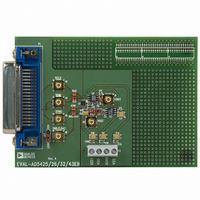
BOARD EVALUATION FOR AD5425
Manufacturer
Analog Devices Inc
Datasheet
1.AD5425YRMZ-REEL.pdf
(28 pages)
Specifications of EVAL-AD5425EBZ
Number Of Dac's
1
Number Of Bits
8
Outputs And Type
1, Differential
Sampling Rate (per Second)
2.47M
Data Interface
Serial
Settling Time
15ns
Dac Type
Current
Voltage Supply Source
Single
Operating Temperature
-40°C ~ 125°C
Utilized Ic / Part
AD5425
Lead Free Status / RoHS Status
Lead free / RoHS Compliant


ADDING GAIN
In applications where the output voltage is required to be
greater than V
amplifier or it can be achieved in a single stage. It is important
to take into consideration the effect of temperature coefficients
of the thin film resistors of the DAC. Simply placing a resistor in
series with the R
erature coefficients and results in larger gain temperature
coefficient errors. Instead, the circuit of Figure 35 is a recom-
mended method of increasing the gain of the circuit. R1, R2,
and R3 should all have similar temperature coefficients, but
they need not match the temperature coefficients of the DAC.
This approach is recommended in circuits where gains of
greater than 1 are required.
DACS USED AS A DIVIDER OR PROGRAMMABLE
GAIN ELEMENT
Current steering DACs are very flexible and lend themselves to
many different applications. If this type of DAC is connected as
the feedback element of an op amp and R
resistor as shown in Figure 36, then the output voltage is
inversely proportional to the digital input fraction, D.
For D = 1 − 2
As D is reduced, the output voltage increases. For small values
of D, it is important to ensure that the amplifier does not satur-
ate and that the required accuracy is met. For example, an 8-bit
DAC driven with the Binary Code 0x10 (00010000), that is, 16
decimal, in the circuit of Figure 36, should cause the output
voltage to be 16 × V
specification of ±0.5 LSB, then D can in fact have a weight
anywhere in the range 15.5/256 to 16.5/256. Therefore, the
possible output voltage is in the range of 15.5 V
an error of 3%, even though the DAC itself has a maximum
error of 0.2%.
V
IN
NOTES:
1. ADDITIONAL PINS OMITTED FOR CLARITY.
2. C1 PHASE COMPENSATION (1pF TO 2pF) MAY BE REQUIRED
V
IF A1 IS A HIGH SPEED AMPLIFIER.
R1
OUT
Figure 35. Increasing the Gain of Current Output DAC
= −V
V
REF
−n
IN
, the output voltage is
IN
, gain can be added with an additional external
FB
/D = −V
resistor causes mismatches in the temp-
GND
V
V
IN
DD
DD
. However, if the DAC has a linearity
IN
R
/(1 − 2
FB
I
I
OUT
OUT
1
2
−n
)
C1
FB
A1
is used as the input
R3
R2
IN
to 16.5 V
GAIN = R2 + R3
R1 = R2R3
R2 + R3
V
OUT
R2
IN
—
Rev. A | Page 17 of 28
DAC leakage current is also a potential error source in divider
circuits. The leakage current must be counterbalanced by an
opposite current supplied from the op amp through the DAC.
Since only a fraction, D, of the current into the V
routed to the I
as follows:
Output Error Voltage Due to DAC Leakage = (Leakage × R)/D
where R is the DAC resistance at the V
leakage current of 10 nA, R = 10 kΩ. With a gain (that is, 1/D)
of 16 the error voltage is 1.6 mV.
REFERENCE SELECTION
When selecting a reference for use with the AD5425 current
output DAC, pay attention to the reference’s output voltage
temperature coefficient specification. This parameter not only
affects the full-scale error, but can also affect the linearity (INL
and DNL) performance. The reference temperature coefficient
should be consistent with the system accuracy specifications.
For example, an 8-bit system required to hold its overall
specification to within 1 LSB over the temperature range 0°C to
50°C dictates that the maximum system drift with temperature
should be less than 78 ppm/°C. A 12-bit system with the same
temperature range to overall specification within 2 LSB requires
a maximum drift of 10 ppm/°C. By choosing a precision
reference with a low output temperature coefficient, this error
source can be minimized. Table 7 suggests some of the
references available from Analog Devices that are suitable for
use with this range of current output DACs.
V
Figure 36. Current Steering DAC Used as a Divider or
NOTE:
1. ADDITIONAL PINS OMITTED FOR CLARITY.
IN
OUT
I
OUT
1 terminal, the output voltage has to change
1
Programmable Gain Element
R
FB
GND
V
V
DD
DD
V
REF
REF
terminal. For a DAC
V
OUT
REF
terminal is
AD5425
Related parts for EVAL-AD5425EBZ
Image
Part Number
Description
Manufacturer
Datasheet
Request
R


Part Number:
Description:
BOARD EVAL FOR SI270X-A
Manufacturer:
Silicon Laboratories Inc
Datasheet:

Part Number:
Description:
BUCK CONV REF DESIGN KIT IP1201
Manufacturer:
International Rectifier
Datasheet:
Part Number:
Description:
BOARD DEMO SYNC DUAL BUCK CNVTER
Manufacturer:
International Rectifier
Datasheet:
Part Number:
Description:
BOARD DEMO SYNC BUCK CONVETER
Manufacturer:
International Rectifier
Datasheet:

Part Number:
Description:
EVALBOARD/EB Omnidirectional microphone - Analog
Manufacturer:
Analog Devices
Datasheet:
Part Number:
Description:
EVALBOARD/EB Omnidirectional microphone - Analog
Manufacturer:
Analog Devices
Datasheet:


Part Number:
Description:
BOARD EVAL LED DRIVER LT3756
Manufacturer:
Linear Technology
Datasheet:

Part Number:
Description:
BOARD EVAL FOR AD7741/7742
Manufacturer:
Analog Devices Inc
Datasheet:

Part Number:
Description:
±1.7g Dual-Axis IMEMS Accelerometer Evaluation Board
Manufacturer:
Analog Devices Inc
Datasheet:

Part Number:
Description:
IC MULTIPLIER ANALOG 8-SOIC T/R
Manufacturer:
Analog Devices Inc
Datasheet:

Part Number:
Description:
IC ANALOG MULTIPLIER 8-DIP
Manufacturer:
Analog Devices Inc
Datasheet:
Part Number:
Description:
IC ANALOG MULTIPLIER 8-SOIC
Manufacturer:
Analog Devices Inc
Datasheet:
Part Number:
Description:
IC ANALOG MULTIPLIER 8-DIP
Manufacturer:
Analog Devices Inc
Datasheet: