EVAL-AD5425EBZ Analog Devices Inc, EVAL-AD5425EBZ Datasheet - Page 18
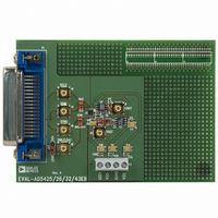
EVAL-AD5425EBZ
Manufacturer Part Number
EVAL-AD5425EBZ
Description
BOARD EVALUATION FOR AD5425
Manufacturer
Analog Devices Inc
Datasheet
1.AD5425YRMZ-REEL.pdf
(28 pages)
Specifications of EVAL-AD5425EBZ
Number Of Dac's
1
Number Of Bits
8
Outputs And Type
1, Differential
Sampling Rate (per Second)
2.47M
Data Interface
Serial
Settling Time
15ns
Dac Type
Current
Voltage Supply Source
Single
Operating Temperature
-40°C ~ 125°C
Utilized Ic / Part
AD5425
Lead Free Status / RoHS Status
Lead free / RoHS Compliant


AD5425
AMPLIFIER SELECTION
The primary requirement for the current-steering mode is an
amplifier with low input bias currents and low input offset vol-
tage. The input offset voltage of an op amp is multiplied by the
variable gain (due to the code dependent output resistance of
the DAC) of the circuit. A change in this noise gain between
two adjacent digital fractions produces a step change in the
output voltage due to the amplifier’s input offset voltage. This
output voltage change is superimposed on the desired change in
output between the two codes and gives rise to a differential
linearity error, which if large enough, could cause the DAC to
be nonmonotonic.
The input bias current of an op amp also generates an offset at
the voltage output as a result of the bias current flowing in the
feedback resistor, R
low enough to prevent any significant errors.
Table 7. Suitable ADI Precision References
Part No.
ADR01
ADR01
ADR02
ADR02
ADR03
ADR03
ADR06
ADR06
ADR431
ADR435
ADR391
ADR395
Table 8. Suitable Precision ADI Op Amps
Part No.
OP97
OP1177
AD8551
AD8603
AD8628
Table 9. Suitable High Speed ADI Op Amps
Part No.
AD8065
AD8021
AD8038
AD9631
Output Voltage (V)
10
10
5
5
2.5
2.5
3
3
2.5
5
2.5
5
Supply Voltage (V)
±2 to ±20
±2.5 to ±15
2.7 to 5
1.8 to 6
2.7 to 6
Supply Voltage (V)
5 to 24
±2.5 to ±12
3 to 12
±3 to ±6
FB
. Most op amps have input bias currents
Initial Tolerance (%)
0.05
0.05
0.06
0.06
0.10
0.10
0.10
0.10
0.04
0.04
0.16
0.10
V
25
60
5
50
5
BW @ ACL (MHz)
145
490
350
320
OS
(Max) (μV)
I
0.1
2
0.05
0.001
0.1
B
B
(Max) (nA)
Slew Rate (V/μs)
180
120
425
1300
Temp Drift (ppm/°C)
3
9
3
9
3
9
3
9
3
3
9
9
Rev. A | Page 18 of 28
0.1 Hz to 10 Hz
Noise (μV p-p)
0.5
0.4
1
2.3
0.5
Common-mode rejection of the op amp is important in voltage
switching circuits, since it produces a code dependent error at
the voltage output of the circuit. Most op amps have adequate
common-mode rejection for use at an 8-bit resolution.
Provided the DAC switches are driven from true wideband low
impedance sources (V
quently, the slew rate and settling time of a voltage switching
DAC circuit is determined largely by the output op amp. To
obtain minimum settling time in this configuration, it is impor-
tant to minimize capacitance at the V
node in this application) of the DAC. This is done by using low
inputs capacitance buffer amplifiers and careful board design.
Most single-supply circuits include ground as part of the analog
signal range, which in turns requires an amplifier that can
handle rail-to-rail signals. There is a large range of single-supply
amplifiers available from Analog Devices.
V
1500
3000
10000
1000
OS
(Max) (μV)
I
1
1
1
1
1
1
1
1
0.8
0.8
0.12
0.12
SS
(mA)
IN
Output Noise (μV p-p)
20
20
10
10
6
6
10
10
3.5
8
5
8
Supply Current (μA)
600
500
975
50
850
and AGND), they settle quickly. Conse-
I
6000
10500
750
7000
B
B
(Max) (nA)
REF
node (voltage output
SOIC-8, SC70-5
Package
SOIC-8, SOT-23,MSOP
SOIC-8, MSOP
SOIC-8
Package
SOIC-8
TSOT-23, SC70
SOIC-8
TSOT-23, SC70
SOIC-8
TSOT-23, SC70
SOIC-8
TSOT-23, SC70
SOIC-8
SOIC-8
TSOT-23
TSOT-23
Package
SOIC-8
MSOP, SOIC-8
MSOP, SOIC-8
TSOT
TSOT, SOIC-8
Related parts for EVAL-AD5425EBZ
Image
Part Number
Description
Manufacturer
Datasheet
Request
R


Part Number:
Description:
BOARD EVAL FOR SI270X-A
Manufacturer:
Silicon Laboratories Inc
Datasheet:

Part Number:
Description:
BUCK CONV REF DESIGN KIT IP1201
Manufacturer:
International Rectifier
Datasheet:
Part Number:
Description:
BOARD DEMO SYNC DUAL BUCK CNVTER
Manufacturer:
International Rectifier
Datasheet:
Part Number:
Description:
BOARD DEMO SYNC BUCK CONVETER
Manufacturer:
International Rectifier
Datasheet:

Part Number:
Description:
EVALBOARD/EB Omnidirectional microphone - Analog
Manufacturer:
Analog Devices
Datasheet:
Part Number:
Description:
EVALBOARD/EB Omnidirectional microphone - Analog
Manufacturer:
Analog Devices
Datasheet:


Part Number:
Description:
BOARD EVAL LED DRIVER LT3756
Manufacturer:
Linear Technology
Datasheet:

Part Number:
Description:
BOARD EVAL FOR AD7741/7742
Manufacturer:
Analog Devices Inc
Datasheet:

Part Number:
Description:
±1.7g Dual-Axis IMEMS Accelerometer Evaluation Board
Manufacturer:
Analog Devices Inc
Datasheet:

Part Number:
Description:
IC MULTIPLIER ANALOG 8-SOIC T/R
Manufacturer:
Analog Devices Inc
Datasheet:

Part Number:
Description:
IC ANALOG MULTIPLIER 8-DIP
Manufacturer:
Analog Devices Inc
Datasheet:
Part Number:
Description:
IC ANALOG MULTIPLIER 8-SOIC
Manufacturer:
Analog Devices Inc
Datasheet:
Part Number:
Description:
IC ANALOG MULTIPLIER 8-DIP
Manufacturer:
Analog Devices Inc
Datasheet: