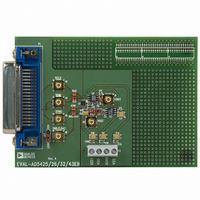
EVAL-AD5425EBZ Analog Devices Inc, EVAL-AD5425EBZ Datasheet - Page 20
EVAL-AD5425EBZ
Manufacturer Part Number
EVAL-AD5425EBZ
Description
BOARD EVALUATION FOR AD5425
Manufacturer
Analog Devices Inc
Datasheet
1.AD5425YRMZ-REEL.pdf
(28 pages)
Specifications of EVAL-AD5425EBZ
Number Of Dac's
1
Number Of Bits
8
Outputs And Type
1, Differential
Sampling Rate (per Second)
2.47M
Data Interface
Serial
Settling Time
15ns
Dac Type
Current
Voltage Supply Source
Single
Operating Temperature
-40°C ~ 125°C
Utilized Ic / Part
AD5425
Lead Free Status / RoHS Status
Lead free / RoHS Compliant


AD5425
ADSP-BF5xx-to-AD5425 Interface
The ADSP-BF5xx family of processors has an SPI-compatible
port that enables the processor to communicate with SPI-
compatible devices. A serial interface between the ADSP-BF5xx
and the AD5425 DAC is shown in Figure 40. In this configura-
tion, data is transferred through the MOSI (master output/slave
input) pin. SYNC is driven by the SPI chip select pin, which is a
reconfigured programmable flag pin.
The ADSP-BF5xx processor incorporates channel synchronous
serial ports (SPORT). A serial interface between the DAC and
the DSP SPORT is shown in Figure 41. When the SPORT is
enabled, initiate transmission by writing a word to the Tx
register. The data is clocked out on each rising edge of the DSP’s
serial clock and clocked into the DAC’s input shift register on
the falling edge of its SCLK. The DAC output is updated by
using the transmit frame synchronization (TFS) line to provide
a SYNC signal.
1
1
ADDITIONAL PINS OMITTED FOR CLARITY.
ADDITIONAL PINS OMITTED FOR CLARITY.
ADSP-BF5xx
ADSP-BF5xx
SPIxSEL
Figure 40. ADSP-BF5xx-to-AD5425 Interface
Figure 41. ADSP-BF5xx-to-AD5425 Interface
SCLK
MOSI
SCK
1
1
TFS
DT
SYNC
SDIN
SCLK
SYNC
SDIN
SCLK
AD5425
AD5425
1
1
Rev. A | Page 20 of 28
80C51/80L51-to-AD5425 Interface
A serial interface between the DAC and the 8051 is shown in
Figure 42. TxD of the 8051 drives SCLK of the DAC serial
interface, while RxD drives the serial data line, D
programmable pin on the serial port that drives SYNC . When
data is transmitted to the switch, P3.3 is taken low. The 80C51/
80L51 transmits data in 8-bit bytes, which fits the AD5425 since
it only requires an 8-bit word. Data on RxD is clocked out of the
microcontroller on the rising edge of TxD and is valid on the
falling edge. As a result, no glue logic is required between the
DAC and microcontroller interface. P3.3 is taken high at the
completion of this cycle. The 8051 provides the LSB of its SBUF
register as the first bit in the data stream. The DAC input reg-
ister requires that the MSB is the first bit received. The transmit
routine should take this into account.
MC68HC11 Interface-to-AD5425 Interface
Figure 43 shows an example of a serial interface between the
DAC and the MC68HC11 microcontroller. The serial
peripheral interface (SPI) on the MC68HC11 is configured for
master mode (MSTR = 1), clock polarity bit (CPOL) = 0, and
the clock phase bit (CPHA) = 1. The SPI is configured by
writing to the SPI control register (SPCR) (see the MC68HC11
user manual). SCK of the MC68HC11 drives the SCLK of the
DAC interface, the MOSI output drives the serial data line, D
of the AD5425. The SYNC signal is derived from a port line,
PC7. When data is being transmitted to the AD5425, the SYNC
line is taken low (PC7). Data appearing on the MOSI output is
valid on the falling edge of SCK. Serial data from the
MC68HC11 is transmitted in 8-bit bytes with only 8 falling
clock edges occurring in the transmit cycle. Data is transmitted
MSB first. PC7 is taken high at the end of the write.
1
1
ADDITIONAL PINS OMITTED FOR CLARITY.
ADDITIONAL PINS OMITTED FOR CLARITY.
MC68HC11
8051
1
Figure 43. 68HC11/68L11-to-AD5425 Interface
Figure 42. 80C51/80L51-to-AD5425 Interface
MOSI
1
SCK
RxD
P1.1
TxD
PC7
SCLK
SDIN
SYNC
SYNC
SCLK
SDIN
AD5425
AD5425
IN
. P3.3 is a bit-
1
1
IN
,
Related parts for EVAL-AD5425EBZ
Image
Part Number
Description
Manufacturer
Datasheet
Request
R


Part Number:
Description:
BOARD EVAL FOR SI270X-A
Manufacturer:
Silicon Laboratories Inc
Datasheet:

Part Number:
Description:
BUCK CONV REF DESIGN KIT IP1201
Manufacturer:
International Rectifier
Datasheet:
Part Number:
Description:
BOARD DEMO SYNC DUAL BUCK CNVTER
Manufacturer:
International Rectifier
Datasheet:
Part Number:
Description:
BOARD DEMO SYNC BUCK CONVETER
Manufacturer:
International Rectifier
Datasheet:

Part Number:
Description:
EVALBOARD/EB Omnidirectional microphone - Analog
Manufacturer:
Analog Devices
Datasheet:
Part Number:
Description:
EVALBOARD/EB Omnidirectional microphone - Analog
Manufacturer:
Analog Devices
Datasheet:


Part Number:
Description:
BOARD EVAL LED DRIVER LT3756
Manufacturer:
Linear Technology
Datasheet:

Part Number:
Description:
BOARD EVAL FOR AD7741/7742
Manufacturer:
Analog Devices Inc
Datasheet:

Part Number:
Description:
±1.7g Dual-Axis IMEMS Accelerometer Evaluation Board
Manufacturer:
Analog Devices Inc
Datasheet:

Part Number:
Description:
IC MULTIPLIER ANALOG 8-SOIC T/R
Manufacturer:
Analog Devices Inc
Datasheet:

Part Number:
Description:
IC ANALOG MULTIPLIER 8-DIP
Manufacturer:
Analog Devices Inc
Datasheet:
Part Number:
Description:
IC ANALOG MULTIPLIER 8-SOIC
Manufacturer:
Analog Devices Inc
Datasheet:
Part Number:
Description:
IC ANALOG MULTIPLIER 8-DIP
Manufacturer:
Analog Devices Inc
Datasheet: