IRPLLED1 International Rectifier, IRPLLED1 Datasheet - Page 15
IRPLLED1
Manufacturer Part Number
IRPLLED1
Description
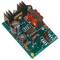
BOARD EVALUATION FOR IRS2540PBF
Manufacturer
International Rectifier
Specifications of IRPLLED1
Current - Output / Channel
1.5A
Outputs And Type
1, Non-Isolated
Voltage - Output
24V
Features
Dimmable
Voltage - Input
50 ~ 170V
Utilized Ic / Part
IRS2540PBF
Core Chip
IRS2540, IRS2541, IRS25401
Topology
Buck (Step Down)
No. Of Outputs
1
Output Current
1.5A
Output Voltage
500mV
Dimming Control Type
PWM
Development Tool Type
Hardware - Eval/Demo Board
Lead Free Status / RoHS Status
Contains lead / RoHS compliant by exemption


A detailed evaluation of system needs and cost should be performed prior to choosing a MOSFET or diode for the
low side. Although a diode is cheaper, in certain cases the associated power losses may require a heatsink,
nullifying the cost reduction of using a diode. Likewise there are conditions where a MOSFET may prove less
efficient, in which case more money will be spent on the MOSFET as well as the heatsink if required. The
evaluation board is provided with a freewheeling diode and the footprint for a low side MOSFET has been provided
to replace the diode with a MOSFET if required. It is not recommended to replace the diode with a MOSFET for the
1A and 1.5A operation because of the associated reverse recovery power losses.
In terms of selecting the correct MOSFET, it is best to use a part with RDSon low as possible. MOSFET parameters
degrade as the voltage ratings go up. Therefore, if a 600V MOSFET is used in a 200V application, extra losses may
be incurred due to a component that far exceeds the requirements. If using two MOSFETs the next parameter to be
considered is the reverse recovery time. Obviously MOSFETs will not have a reverse recovery time comparable to
diodes but a reverse recovery time in the order of 150 to 200ns is possible. The two remaining parameters to
consider are direct trade-offs of each other, on resistance and gate charge. If the MOSFET has a relatively low gate
capacitance, the die size will be small, which will result in a larger on resistance that could potentially be a problem
for high current applications. On the other hand, if the MOSFET has a larger gate capacitance, the die will be
relatively large and the part will have a lower on resistance. In this case more current is needed to turn on the
MOSFET therefore requiring more VCC current in the IRS2540 and resulting in hgigher losses. There has to be a
direct compromise between the two. Typically the best solution is a MOSFET with a relatively low RDSon and a
medium sized gate capacitance, much like the device chosen for this application
6. VCC Supply
Since the IRS2450/1 is rated for 200V/600V VBUS can rvary considerably in different applications. If a simple
supply resistor from VBUS is used for VCC it will experience high power losses at higher bus voltages. For higher
voltage applications therefore an alternate V CC supply scheme utilizing a resistor feed-back (RS2) from the output
needs to be implemented, as seen in Fig. 1 and Fig. 16. This solution is limited to applications where the LED string
voltage exceeds the voltage required to drive VCC, which is about 13V to guarantee good operation.
The resistance between VBUS and V CC (RS1) should be large enough to minimize the current sourced directly
from the input voltage line. Through this supply resistor a current will flow to charge the V CC capacitor. Once the
capacitor is charged up to the V CCUV+ threshold, the IRS2540/1 begins to operate activating the LO and HO
outputs. After the first few cycles of switching the resistor RS2 connected between the output and V CC will take
over and source current for VCC from the output. The RS2 resistor provided in the evaluation board has been
designed for an output of roughly 20V. If a higher output voltage is desired, RS2 will need to be redesigned and
adjusted accordingly. Conversely, if the output voltage is below 20V the value of RS2 may need to be reduced in
order to supply sufficient voltage to VCC.
A 10uF capacitor has been used at VCC of the IRS2540, which removes most low frequency ripple that could
originate from VBUS due to a rectified voltage waveform.
If the input and output voltages are defined for the evaluation board, enough information is provided to calculate
values for RS1, RS2, and RS3 (see Fig. 23 for component definition). All three supply resistors were chosen to be
1W devices since they source all current to the chip. Efficiency can be improved by optimizing these values for
specific applications.
By making each component 1W, the work in supplying VCC can be split up equally making it a more robust
solution instead of relying entirely on one component. This also allows the chip to turn on at a lower bus voltage.
Assuming that a 14V external zener diode will be used on Vcc, exact values of RS1, RS2, and RS3 are calculated as
follows (values calculated to operate the components just below half their rated power):
RD-0608
15
www.irf.com
Related parts for IRPLLED1
Image
Part Number
Description
Manufacturer
Datasheet
Request
R

Part Number:
Description:
SCHOTTKY RECTIFIER
Manufacturer:
International Rectifier Corp.
Datasheet:
Part Number:
Description:
SCHOTTKY RECTIFIER
Manufacturer:
International Rectifier Corp.
Datasheet:
Part Number:
Description:
SCHOTTKY RECTIFIER
Manufacturer:
International Rectifier Corp.
Datasheet:
Part Number:
Description:
SCHOTTKY RECTIFIER
Manufacturer:
International Rectifier Corp.
Datasheet:
Part Number:
Description:
SCHOTTKY RECTIFIER
Manufacturer:
International Rectifier Corp.
Datasheet:
Part Number:
Description:
SCHOTTKY RECTIFIER
Manufacturer:
International Rectifier Corp.
Datasheet:
Part Number:
Description:
SCHOTTKY RECTIFIER
Manufacturer:
International Rectifier Corp.
Datasheet:
Part Number:
Description:
SCHOTTKY RECTIFIER
Manufacturer:
International Rectifier Corp.
Datasheet:
Part Number:
Description:
SCHOTTKY RECTIFIER
Manufacturer:
International Rectifier Corp.
Datasheet:
Part Number:
Description:
SCHOTTKY RECTIFIER
Manufacturer:
International Rectifier Corp.
Datasheet:
Part Number:
Description:
SCHOTTKY RECTIFIER
Manufacturer:
International Rectifier Corp.
Datasheet:
Part Number:
Description:
SCHOTTKY RECTIFIER
Manufacturer:
International Rectifier Corp.
Datasheet:
Part Number:
Description:
SCHOTTKY RECTIFIER
Manufacturer:
International Rectifier Corp.
Datasheet:
Part Number:
Description:
SCHOTTKY RECTIFIER
Manufacturer:
International Rectifier Corp.
Datasheet:
Part Number:
Description:
SCHOTTKY RECTIFIER
Manufacturer:
International Rectifier Corp.
Datasheet: