LM3552SDEV National Semiconductor, LM3552SDEV Datasheet - Page 11
LM3552SDEV
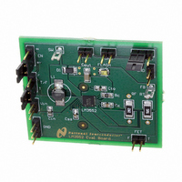
Manufacturer Part Number
LM3552SDEV
Description
BOARD EVALUATION LM3552SD
Manufacturer
National Semiconductor
Series
PowerWise®r
Specifications of LM3552SDEV
Current - Output / Channel
700mA
Outputs And Type
1, Non-Isolated
Voltage - Output
4 V
Features
Flash Timeout Protection
Voltage - Input
2.7 ~ 5.5V
Utilized Ic / Part
LM3552
Core Chip
LM3552
Topology
Boost
No. Of Outputs
1
Output Current
1A
Input Voltage
2.7V To 5.5V
Development Tool Type
Hardware - Eval/Demo Board
Mcu Supported Families
LM3552
Lead Free Status / RoHS Status
Not applicable / Not applicable


DIODE SELECTION
The output diode for a boost regulator must be chosen cor-
rectly depending on the output voltage and output current.
The output diode must have a reverse voltage rating equal to
or greater than the output voltage used. The average current
rating must be greater than the maximum load current ex-
pected, and the peak current rating must be greater than the
peak inductor current. Using Schottky diodes with lower for-
ward voltage drop will decrease power dissipation and in-
crease efficiency.
CAPACITOR SELECTION
Input Capacitor
An input capacitor is required to reduce the input ripple and
noise for proper operation of the regulator. The size used is
dependant on the application and board layout. If the regula-
tor will be loaded uniformly, with very little load changes, and
at lower current outputs, the input capacitor size can often be
reduced. The size can also be reduced if the input of the reg-
ulator is very close to the source output. The size will generally
need to be larger for applications where the regulator is sup-
plying nearly the maximum rated output or if large load steps
are expected. A minimum value of 10µF should be used under
normal operating condtions while a 10-22µF capacitor may
be required for higher power and dynamic loads. Larger val-
ues and/or lower ESR may be needed if the application
requires very low ripple on the input source voltage.
Output Capacitor
A minimum output capacitor value of 4.7µF (Sharp LED) and
10µF (Lumiled) is recommended and may be increased to a
larger value. The ESR of the output capacitor is important
because it determines the peak to peak output voltage ripple
according to the approximate equation:
After choosing the output capacitor you can determine a pole-
zero pair introduced into the control loop by the following
equations:
The zero created by the ESR of the output capacitor is gen-
erally at a very high frequency if the ESR is small. If low ESR
capacitors are used it can be neglected. The output capacitor
pole information is useful in selecting the proper compensa-
tion components and is discussed in the COMPENSATION
COMPONENTS section of the datasheet.
Capacitor Properties
Surface-mount multi-layer ceramic capacitors are recom-
mended for both the input and output capacitors. These ca-
pacitors are small, inexpensive and have very low equivalent
series resistance (ESR <20mΩ typ.). Tantalum capacitors,
OS-CON capacitors, and aluminum electrolytic capacitors are
not recommended for use with the LM3551/2 due to their high
ESR, as compared to ceramic capacitors.
For most applications, ceramic capacitors with X7R or X5R
temperature characteristic are preferred for use with the
LM3551/2. These capacitors have tight capacitance tolerance
ΔV
OUT
≊
2 × ΔI
L
× R
ESR
(in Volts)
11
(as good as ±10%) and hold their value over temperature
(X7R: ±15% over -55°C to 125°C; X5R: ±15% over -55°C to
85°C).
Capacitors with Y5V or Z5U temperature characteristic are
generally not recommended for use with the LM3551/2. Ca-
pacitors with these temperature characteristics typically have
wide capacitance tolerance (+80%, -20%) and vary signifi-
cantly over temperature (Y5V: +22%, -82% over -30°C to
+85°C range; Z5U: +22%, -56% over +10°C to +85°C range).
Under some conditions, a nominal 1µF Y5V or Z5U capacitor
could have a capacitance of only 0.1µF. Such deviation is
likely to cause Y5V and Z5U capacitors to fail to meet the
minimum capacitance requirements of the LM3551/2.
The minimum voltage rating acceptable for the input capacitor
is 6.3V (10V recommended) and 16V for the output capacitor.
In applications that have DC operating points near the maxi-
mum voltage rating of the ceramic capacitor, larger capacitor
values may be required to compensate for capacitance loss
due to capacitor voltage coefficient. See the capacitor
manufacturer's datasheet for DC bias performance.
COMPENSATION
DC Gain and Open-Loop Gain
Since the control stage of the converter forms a complete
feedback loop with the power components, it forms a closed-
loop system that must be stabilized to avoid positive feedback
and instability. A value for open-loop DC gain will be required,
from which you can calculate, or place, poles and zeros to
determine the crossover frequency and the phase margin. A
high phase margin (greater than 45°) is desired for the best
stability and transient response. For the purpose of stabilizing
the LM3551/2, choosing a crossover point well below where
the right half plane zero is located will ensure sufficient phase
margin.
To ensure a bandwidth of ½ or less of the frequency of the
RHP zero, calculate the open-loop DC gain, A
value is known, you can calculate the crossover visually by
placing a −20dB/decade slope at each pole, and a +20dB/
decade slope for each zero. The point at which the gain plot
crosses unity gain, or 0dB, is the crossover frequency. If the
crossover frequency is less than ½ the RHP zero, the phase
margin should be high enough for stability. The equation for
A
calculation:
DC
is given below with additional equations required for the
mc
≊
0.072 × fs (in V/s)
DC
www.national.com
. After this
Related parts for LM3552SDEV
Image
Part Number
Description
Manufacturer
Datasheet
Request
R


Part Number:
Description:
Precision Centigrade Temperature Sensors
Manufacturer:
National Semiconductor

Part Number:
Description:
Precision Centigrade Temperature Sensors
Manufacturer:
National Semiconductor Corporation
Datasheet:
Part Number:
Description:
National Semiconductor [8-Bit D/A Converter]
Manufacturer:
National Semiconductor
Datasheet:
Part Number:
Description:
National Semiconductor [Media Coprocessor]
Manufacturer:
National Semiconductor
Datasheet:
Part Number:
Description:
Digitally Controlled Tone and Volume Circuit with Stereo Audio Power Amplifier, Microphone Preamp Stage and National 3D Sound
Manufacturer:
National Semiconductor
Datasheet:
Part Number:
Description:
Digitally Controlled Tone and Volume Circuit with Stereo Audio Power Amplifier, Microphone Preamp Stage and National 3D Sound
Manufacturer:
National Semiconductor
Datasheet:
Part Number:
Description:
AC97 Rev 2 Codec with Sample Rate Conversion and National 3D Sound
Manufacturer:
National Semiconductor
Part Number:
Description:
Manufacturer:
National Semiconductor
Datasheet:
Part Number:
Description:
Manufacturer:
National Semiconductor
Datasheet:
Part Number:
Description:
General Purpose, Low Voltage, Low Power, Rail-to-Rail Output Operational Amplifiers
Manufacturer:
National Semiconductor
Datasheet:
Part Number:
Description:
8-bit 20 MSPS flash A/D converter.
Manufacturer:
National Semiconductor
Datasheet:
Part Number:
Description:
Low Noise Quad Operational Amplifier
Manufacturer:
National Semiconductor
Datasheet:
Part Number:
Description:
Quad Differential Line Receivers
Manufacturer:
National Semiconductor
Datasheet: