LM3552SDEV National Semiconductor, LM3552SDEV Datasheet - Page 3
LM3552SDEV
Manufacturer Part Number
LM3552SDEV
Description
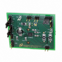
BOARD EVALUATION LM3552SD
Manufacturer
National Semiconductor
Series
PowerWise®r
Specifications of LM3552SDEV
Current - Output / Channel
700mA
Outputs And Type
1, Non-Isolated
Voltage - Output
4 V
Features
Flash Timeout Protection
Voltage - Input
2.7 ~ 5.5V
Utilized Ic / Part
LM3552
Core Chip
LM3552
Topology
Boost
No. Of Outputs
1
Output Current
1A
Input Voltage
2.7V To 5.5V
Development Tool Type
Hardware - Eval/Demo Board
Mcu Supported Families
LM3552
Lead Free Status / RoHS Status
Not applicable / Not applicable


I
I
I
V
I
g
A
D
f
I
I
I
I
R
I
R
I
R
Th
Q
SD
CL
FB
sw
SDPIN
ENPIN
T/FPIN
L-SW
L-T
L-F
m
FB
V
MAX
DSON-SW
DSON-T
DSON-F
Absolute Maximum Ratings
2)
If Military/Aerospace specified devices are required,
please contact the National Semiconductor Sales Office/
Distributors for availability and specifications.
ESD Caution Notice
ESD precautions. Failure to observe proper ESD handling techniques can result in damage to the device.
Electrical Characteristics
Limits in standard typeface are for T
(-40°C
1) with: V
Symbol
SD/EN
V
SW pin: Voltage to GND
FB pin: Voltage to GND
V
SD,T/F pins: Voltage to GND
FET-T, FET-F: Voltage to GND
Continuous Power Dissipation
Junction Temperature (T
Storage Temperature Range
Maximum Lead Temperature
(Soldering)
ESD
Human Body Model
(Note
(Note
IN
C
pin: Voltage to GND
pin: Voltage to GND
Rating(Note
11) Switch Current Limit
13) Feedback Pin Bias Current
≤
T
IN
J
= 3.6V, V(SD) = 0V for LM3551 and V(EN) = V
Quiescent Current
Shutdown Current
Feedback Voltage
Error Amp Transconductance ΔI = 5µA
Error Amp Voltage Gain
Maximum Duty Cycle
Switching Frequency
Shutdown Pin Current
(LM3551)
Enable Pin Current
(LM3552)
T/F Pin Current
SW Pin Leakage Current
SW Pin R
FET-T Leakage Current
FET-T R
FET-F Leakage Current
FET-F R
Shutdown/Enable Pin
Threshold
≤
+110°C). Unless otherwise noted, specifications apply to the LM3551 and LM3552 Typical Application Circuit (pg.
5)
DSON
DSON
Parameter
DSON
J-MAX )
(Note
National Semiconductor recommends that all integrated circuits be handled with appropriate
J
= +25° C. Limits in boldface type apply over the full operating junction temperature range
3) Internally Limited
FB = V
V(SD) = V
LM3551
V(EN) = 0V
LM3552
V
(Note
IN
-65°C to +150
1.26V ± 0.3V
= 3.0V
(Note
2,
IN
(Note
(Not Switching)
Note
V
Output High
Conditions
Output Low
IN
150°C
V
1,
I
2.0kV
(Note
V
V
SW
V
L-SW
EN
7.5V
7.5V
T/F
21V
SD
T/F
Note
7V
6V
= 0.5A
4)
= 3.6V
9)
= V
= 0V
= 0V
IN
= 20V
12)
for LM3552, I
IN
3
Operating Ratings
Thermal Properties
Input Voltage Range
SW Voltage Max.
Junction Temperature (T
Range
Ambient Temperature (T
Range
Junction-to-Ambient Thermal
Resistance (θ
Package
LOAD
(Note
(Note
1.2285
= 0A
Min
0.9
1.2
7)
JA
(Note
8)
), SDA14B
(Note
10)
1.265
0.165
6)
A
1.47
2.55
92.5
1.25
0.07
0.98
0.36
J
Typ
135
135
0.1
2.1
3.0
3.0
0.1
0.1
)
50
26
22
)
(Note
1,
1.2915
Max
2.0
5.0
2.3
1.6
0.3
Note
6
6
8
-40°C to +110°C
-40°C to +85°C
2)
2.7V to 5.5V
www.national.com
37.3°C/W
Units
µmho
MHz
V/V
mA
µA
nA
µA
µA
nA
µA
µA
µA
%
Ω
Ω
Ω
20V
A
V
V
Related parts for LM3552SDEV
Image
Part Number
Description
Manufacturer
Datasheet
Request
R


Part Number:
Description:
Precision Centigrade Temperature Sensors
Manufacturer:
National Semiconductor

Part Number:
Description:
Precision Centigrade Temperature Sensors
Manufacturer:
National Semiconductor Corporation
Datasheet:
Part Number:
Description:
National Semiconductor [8-Bit D/A Converter]
Manufacturer:
National Semiconductor
Datasheet:
Part Number:
Description:
National Semiconductor [Media Coprocessor]
Manufacturer:
National Semiconductor
Datasheet:
Part Number:
Description:
Digitally Controlled Tone and Volume Circuit with Stereo Audio Power Amplifier, Microphone Preamp Stage and National 3D Sound
Manufacturer:
National Semiconductor
Datasheet:
Part Number:
Description:
Digitally Controlled Tone and Volume Circuit with Stereo Audio Power Amplifier, Microphone Preamp Stage and National 3D Sound
Manufacturer:
National Semiconductor
Datasheet:
Part Number:
Description:
AC97 Rev 2 Codec with Sample Rate Conversion and National 3D Sound
Manufacturer:
National Semiconductor
Part Number:
Description:
Manufacturer:
National Semiconductor
Datasheet:
Part Number:
Description:
Manufacturer:
National Semiconductor
Datasheet:
Part Number:
Description:
General Purpose, Low Voltage, Low Power, Rail-to-Rail Output Operational Amplifiers
Manufacturer:
National Semiconductor
Datasheet:
Part Number:
Description:
8-bit 20 MSPS flash A/D converter.
Manufacturer:
National Semiconductor
Datasheet:
Part Number:
Description:
Low Noise Quad Operational Amplifier
Manufacturer:
National Semiconductor
Datasheet:
Part Number:
Description:
Quad Differential Line Receivers
Manufacturer:
National Semiconductor
Datasheet: