LM3552SDEV National Semiconductor, LM3552SDEV Datasheet - Page 4
LM3552SDEV
Manufacturer Part Number
LM3552SDEV
Description
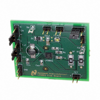
BOARD EVALUATION LM3552SD
Manufacturer
National Semiconductor
Series
PowerWise®r
Specifications of LM3552SDEV
Current - Output / Channel
700mA
Outputs And Type
1, Non-Isolated
Voltage - Output
4 V
Features
Flash Timeout Protection
Voltage - Input
2.7 ~ 5.5V
Utilized Ic / Part
LM3552
Core Chip
LM3552
Topology
Boost
No. Of Outputs
1
Output Current
1A
Input Voltage
2.7V To 5.5V
Development Tool Type
Hardware - Eval/Demo Board
Mcu Supported Families
LM3552
Lead Free Status / RoHS Status
Not applicable / Not applicable


www.national.com
Th
UVP
OVP
V
I
V
I
FTO
SS
FTO
SS
Note 1: Absolute Maximum Ratings indicate limits beyond which damage to the component may occur. Operating Ratings are conditions under which operation
of the device is guaranteed. Operating Ratings do not imply guaranteed performance limits. For guaranteed performance limits and associated test conditions,
see the Electrical Characteristics tables.
Note 2: All voltages are with respect to the potential at the GND pin.
Note 3: Internal thermal shutdown circuitry protects the device from permanent damage. Thermal shutdown engages at T
T
Note 4: For detailed soldering specifications and information, please refer to National Semiconductor Application Note: AN-1187 for Recommended Soldering
Profiles.
Note 5: The human body model is a 100pF capacitor discharged through a 1.5kΩ resistor into each pin. (MIL-STD-883 3015.7)
Note 6: Maximum recommended SW pin voltage when the OVP pin is grounded.
Note 7: In applications where high power dissipation and/or poor package thermal resistance is present, the maximum ambient temperature may have to be
derated. Maximum ambient temperature (T
dissipation of the device in the application (P
following equation: T
Note 8: Junction-to-ambient thermal resistance is highly application and board-layout dependent. In applications where high maximum power dissipation exists,
special care must be paid to thermal dissipation issues in board design.
Note 9: Min and Max limits are guaranteed by design, test, or statistical analysis. Typical (Typ) numbers are not guaranteed, but do represent the most likely
norm. Unless otherwise specified, conditions for Typ specifications are: V
Note 10: C
Note 11: Duty cycle affects current limit due to ramp generator.
Note 12: Current limit at 0% duty cycle. See TYPICAL PERFORMANCE section for Switch Current Limit vs. V
Note 13: Bias current flows into FB pin.
Symbol
T/F
J
=120ºC (typ.).
IN
and C
T/F Pin Threshold
Under Voltage Protection
Thresholds
Over Voltage Protection
Thresholds
Flash Timeout trip-point
Flash Timeout Current
Soft-Start Voltage
Soft-Start Current
OUT
A-MAX
,: Low-ESR Surface-Mount Ceramic Capacitors (MLCCs) used in setting electrical characteristics
Parameter
= T
J-MAX-OP
– (θ
JA
A-MAX
× P
D-MAX
D-MAX
) is dependent on the maximum operating junction temperature (T
), and the junction-to-ambient thermal resistance of the part/package in the application (θ
).
On Threshold
Off Threshold
On Threshold
Off Threshold
Output High
Conditions
Output Low
IN
= 3.6V and T
4
A
= 25ºC.
2.25
2.43
11.3
0.99
1.12
1.18
Min
1.2
9.2
10
IN
J-MAX-OP
2.48
2.58
12.4
10.6
1.16
1.25
11.5
Typ
1.4
J
=140ºC (typ.) and disengages at
= 110ºC), the maximum power
Max
2.70
2.77
1.32
1.68
1.32
0.3
14
12
13
JA
), as given by the
Units
µA
µA
V
V
V
V
V
Related parts for LM3552SDEV
Image
Part Number
Description
Manufacturer
Datasheet
Request
R


Part Number:
Description:
Precision Centigrade Temperature Sensors
Manufacturer:
National Semiconductor

Part Number:
Description:
Precision Centigrade Temperature Sensors
Manufacturer:
National Semiconductor Corporation
Datasheet:
Part Number:
Description:
National Semiconductor [8-Bit D/A Converter]
Manufacturer:
National Semiconductor
Datasheet:
Part Number:
Description:
National Semiconductor [Media Coprocessor]
Manufacturer:
National Semiconductor
Datasheet:
Part Number:
Description:
Digitally Controlled Tone and Volume Circuit with Stereo Audio Power Amplifier, Microphone Preamp Stage and National 3D Sound
Manufacturer:
National Semiconductor
Datasheet:
Part Number:
Description:
Digitally Controlled Tone and Volume Circuit with Stereo Audio Power Amplifier, Microphone Preamp Stage and National 3D Sound
Manufacturer:
National Semiconductor
Datasheet:
Part Number:
Description:
AC97 Rev 2 Codec with Sample Rate Conversion and National 3D Sound
Manufacturer:
National Semiconductor
Part Number:
Description:
Manufacturer:
National Semiconductor
Datasheet:
Part Number:
Description:
Manufacturer:
National Semiconductor
Datasheet:
Part Number:
Description:
General Purpose, Low Voltage, Low Power, Rail-to-Rail Output Operational Amplifiers
Manufacturer:
National Semiconductor
Datasheet:
Part Number:
Description:
8-bit 20 MSPS flash A/D converter.
Manufacturer:
National Semiconductor
Datasheet:
Part Number:
Description:
Low Noise Quad Operational Amplifier
Manufacturer:
National Semiconductor
Datasheet:
Part Number:
Description:
Quad Differential Line Receivers
Manufacturer:
National Semiconductor
Datasheet: