CYIL1SM4000-EVAL Cypress Semiconductor Corp, CYIL1SM4000-EVAL Datasheet
CYIL1SM4000-EVAL
Specifications of CYIL1SM4000-EVAL


Related parts for CYIL1SM4000-EVAL

CYIL1SM4000-EVAL Summary of contents
Page 1
... LUPA-4000 Data Sheet LUPA-4000 4M Pixel CMOS Image Sensor Datasheet Cypress Semiconductor Corporation 3901 North First Street Contact: info@Fillfactory.com Document #: 38-05712 Rev.**(Revision 1.2 ) San Jose, CA 95134 408-943-2600 Page ...
Page 2
... Issue Date 1.0 August, 2004 1.0 November, 2004 1.1 November, 2004 1.2 December 23, 2004 Cypress Semiconductor Corporation Contact: info@Fillfactory.com Document #: 38-05712 Rev.**(Revision 1.2 ) Description of changes Origination Correct bias voltages precharge_bias and Pre_load Updated timing diagrams and timing explanation Added Cypress equivalent part numbers, ...
Page 3
... IMING OF THE PIXEL ARRAY 4.2 R EAD OUT OF THE IMAGE SENSOR 4.2.1 X- and Y-addressing.................................................................................29 4.2.2 Reduced Row Overhead Time timing.......................................................32 4.2.2.a Standard timing (200ns)................................................................................................33 4.2.2.b Back-up timing (ROT =100-200 ns).............................................................................33 Cypress Semiconductor Corporation Contact: info@Fillfactory.com Document #: 38-05712 Rev.**(Revision 1.2 ) .................................................................................6 ...................................................................6 .........................................................9 ..........................................................................10 ........................................................................13 ...................................................................15 .................................................................................17 (NDR) ..............................................................17 ...
Page 4
... ONDING PADS 6.4 B .........................................................................................44 ONDING DIAGRAM 7 HANDLING AND SOLDERING PRECAUTIONS ........................................45 8 ORDERING INFORMATION ..........................................................................46 APPENDIX A: LUPA-4000 EVALUATION SYSTEM.........................................47 APPENDIX B: FREQUENTLY ASKED QUESTIONS .....................................48 Cypress Semiconductor Corporation Contact: info@Fillfactory.com Document #: 38-05712 Rev.**(Revision 1.2 ) (SPI) ..............................................................35 3901 North First Street San Jose, CA 95134 408-943-2600 Page ...
Page 5
... Random programmable windowing and sub-sampling modes. • 127-pin PGA package • Binning (Voltage averaging in X-direction) • Programmable read out direction (X and Y) 1.3 Part Number Name LUPA-4000-M CYIL1SM4000AA-GBC (preliminary) Cypress Semiconductor Corporation Contact: info@Fillfactory.com Document #: 38-05712 Rev.**(Revision 1.2 ) Package Monochrome / color ...
Page 6
... Parasitic sensitivity < 1/5000 MTF 64% Power dissipation <200 mWatt Cypress Semiconductor Corporation Contact: info@Fillfactory.com Document #: 38-05712 Rev.**(Revision 1.2 ) Remarks Based on the high fill-factor active pixel sensor technology of FillFactory The resolution and pixel size results 24,6mm optical active area. ...
Page 7
... The sensor is light sensitive between 400 and 1000 nm. The peak 37.5% approximately between 500 and 700 nm. In view of a fill factor of 60%, the QE is thus larger than 60% between 500 and 700 nm. Cypress Semiconductor Corporation Contact: info@Fillfactory.com Document #: 38-05712 Rev.**(Revision 1.2 ) ...
Page 8
... The resulting voltage-electron curve is independent of any parameters. The voltage to electrons conversion gain is 13.5 µV/electron. Note that the upper part of the curve (near saturation) is actually a logarithmic response. Cypress Semiconductor Corporation Contact: info@Fillfactory.com Document #: 38-05712 Rev.**(Revision 1.2 ) 60000 ...
Page 9
... PGA package Power dissipation <200mW <100g Mass Differential Output amplifiers R > External output load C < (< advised Mpixels/sec Number of outputs 2 at 33Mpixels/sec Cypress Semiconductor Corporation Contact: info@Fillfactory.com Document #: 38-05712 Rev.**(Revision 1.2 ) Ω 3901 North First Street San Jose, CA 95134 408-943-2600 Page ...
Page 10
... This device contains circuitry to protect the inputs against damage due to high static voltages or electric fields; however it is recommended that normal precautions be taken to avoid application of any voltages higher than the maximum rated voltages to this high impedance circuit. Cypress Semiconductor Corporation Contact: info@Fillfactory.com Document #: 38-05712 Rev.**(Revision 1.2 ) ...
Page 11
... The starting point of the address is uploadable by means of the Serial- Parallel Interface (SPI). eos_y Clk_y sync_y Clk_x Logic blocks sync_x Figure 3: Block diagram of the image sensor Cypress Semiconductor Corporation Contact: info@Fillfactory.com Document #: 38-05712 Rev.**(Revision 1 chip drivers pixel array 2048 * 2048 Column amplifiers ...
Page 12
... Parasitic Light Sensitivity (PLS), the pixel architecture given in the figure below is implemented. Vpix Reset Figure 4: 6T-pixel architecture This pixel architecture is designed µm to meet the specifications as described in Tables 1, 2 and 3. Cypress Semiconductor Corporation Contact: info@Fillfactory.com Document #: 38-05712 Rev.**(Revision 1.2 ) Vmem Sample 2 pixel pitch ...
Page 13
... Table 5: Frame rate as function of ROI read out and/or sub sampling Image Resolution Frame rate (X*Y) [frames/s] 2048 x 2048 15 31 1024 x 2048 1024 x 1024 62 640 x 480 210 Cypress Semiconductor Corporation Contact: info@Fillfactory.com Document #: 38-05712 Rev.**(Revision 1.2 ) Frame readout Comment time [ms] 67 Full resolution. 32 Subsample in X-direction. 16 ROI read out. ...
Page 14
... This means that the charging on sensor level is fixed and that the sensor cannot be overdriven from externally. In the paragraph on the timing, the operation of the on-chip drivers is explained more in detail. Cypress Semiconductor Corporation Contact: info@Fillfactory.com Document #: 38-05712 Rev.**(Revision 1.2 ) ...
Page 15
... Power dissipation @ 33 MHz Conversion law (*): The internal ADC range will be typ. 50mV lower then the external applied A and A DC_VHIGH DC_VLOW resistors in the ADC. Cypress Semiconductor Corporation Contact: info@Fillfactory.com Document #: 38-05712 Rev.**(Revision 1.2 ) Table 6: ADC specifications Specification 1 – 2V (*) 10 Bits 33 Msamples/s Typ. < ...
Page 16
... Figure 7: In- and external ADC connections The internal resistor R has a value of approximately 300 Ω. ADC This results in the values for the external resistors: Resistor Cypress Semiconductor Corporation Contact: info@Fillfactory.com Document #: 38-05712 Rev.**(Revision 1.2 ) DC_CLOCK Figure 6: ADC timing 2.5V RHIGH_ADC external ...
Page 17
... The initial reset level and all intermediate signals can be recorded. quickly, but a useful signal is obtained from the early samples. For low light levels, one has to use the later or latest samples. Cypress Semiconductor Corporation Contact: info@Fillfactory.com Document #: 38-05712 Rev.**(Revision 1.2 ) ...
Page 18
... On chip we have the ground lines of every module which are kept separately to improve shielding and electrical cross talk between them. Cypress Semiconductor Corporation Contact: info@Fillfactory.com Document #: 38-05712 Rev.**(Revision 1.2 ) ...
Page 19
... Especially the voltage supplies Vpix and Vaa are important to be well noise free. Cypress Semiconductor Corporation Contact: info@Fillfactory.com Document #: 38-05712 Rev.**(Revision 1.2 ) Table 8: Power supplies Typ ...
Page 20
... Vdd and capacitor of 100 nF to Gnd Connect with 25 K muxbus_load Vaa and capacitor of 100 nF to Gnd Connect with 5 K nsf_load Vaa and capacitor of 100 nF to Gnd Cypress Semiconductor Corporation Contact: info@Fillfactory.com Document #: 38-05712 Rev.**(Revision 1.2 ) Related module Ω to Output stage Ω to X-addressing Ω ...
Page 21
... Each biasing signal determines the operation of a corresponding module in the sense that it controls speed and dissipation. Some modules have 2 biasing resistors: one to achieve the high speed and another to minimize power dissipation. Cypress Semiconductor Corporation Contact: info@Fillfactory.com Document #: 38-05712 Rev.**(Revision 1.2 ) Related module Ω ...
Page 22
... Vmem : this signal increases the information on the memory element with a certain offset. This way one can increase the output voltage variation. Vmem changes between Vmem_l (2.5V) and Vmem_h (3.3V). Cypress Semiconductor Corporation Contact: info@Fillfactory.com Document #: 38-05712 Rev.**(Revision 1.2 ) ...
Page 23
... Note that multiple slopes are possible having multiple Reset_ds pulses with a lower Vres_ds level for each pulse given within the same integration time. Cypress Semiconductor Corporation Contact: info@Fillfactory.com Document #: 38-05712 Rev.**(Revision 1.2 ) ...
Page 24
... Temperature diode (2): Apply a forward current of 10-100 µ A and measure the voltage V of the diode with approximately 1,6 mV/°C). • End of scan pulses (do not use to trigger other signals): Cypress Semiconductor Corporation Contact: info@Fillfactory.com Document #: 38-05712 Rev.**(Revision 1.2 ) varies linear with the temperature (V T ...
Page 25
... Eos_y: end of scan signal output signal, indicating when the end of the frame is reached. Is not generated when doing windowing. o Eos_spi: output signal of the SPI to check if the data is transferred correctly through the SPI. Cypress Semiconductor Corporation 3901 North First Street Contact: info@Fillfactory.com Document #: 38-05712 Rev.**(Revision 1.2 ) ...
Page 26
... The LUPA-4000 sensor also can be used in sequential mode (triggered snapshot mode) where readout and integration will be sequentially. Figure 12 shows this sequential timing sequence. Read frame I Integration I Figure 12: Integration and readout sequentially Cypress Semiconductor Corporation Contact: info@Fillfactory.com Document #: 38-05712 Rev.**(Revision 1.2 ) Read frame Integration ...
Page 27
... Falling edge of Precharge is equal or later than falling edge of Vmem. Sample is overlapping with precharge. Rising edge of Vmem is more than 200nsec after rising edge of Sample. Rising edge of reset is equal or later than rising edge of Vmem. Cypress Semiconductor Corporation Contact: info@Fillfactory.com Document #: 38-05712 Rev.**(Revision 1.2 ) Value 5 – ...
Page 28
... Keeping the slow fall times of the corresponding internal generated signals in mind, the minimal integration time is about 2 µ sec. An additional reset pulse of minimum 2 µ sec can be given during integration by asserting Reset_ds to implement the double slope integration mode. Cypress Semiconductor Corporation Contact: info@Fillfactory.com Document #: 38-05712 Rev.**(Revision 1.2 ) ...
Page 29
... If a Sync_y pulse is given before the end of the frame is reached, only a part of the frame will be read. To obtain a correct initialisation Sync_y must contain at least 1 rising edge of Clock_y when it is active. Cypress Semiconductor Corporation Contact: info@Fillfactory.com Document #: 38-05712 Rev.**(Revision 1.2 ) ...
Page 30
... As soon as a new line is selected, it has to be read out by the output amplifiers. Before the pixels of the selected line can be multiplexed onto the output amplifiers, one has to wait a certain time, indicated as the ROT or Row overhead time shown in Cypress Semiconductor Corporation Contact: info@Fillfactory.com Document #: 38-05712 Rev ...
Page 31
... In this figure the pixel clock has a frequency of 50MHz, which would result in a pixel rate of 100 Msamples/sec. Figure 17 shows the relation between the applied Clock_x and the output signal. Cypress Semiconductor Corporation Contact: info@Fillfactory.com Document #: 38-05712 Rev.**(Revision 1.2 ) ...
Page 32
... The row overhead time is the time between the selection of lines that one has to wait to get the data stable at the column amplifiers. This row overhead time is a loss in time, which should be reduced as much as possible. Cypress Semiconductor Corporation Contact: info@Fillfactory.com Document #: 38-05712 Rev.**(Revision 1.2 ) Pixel2… ...
Page 33
... Sh_col signal and a “voltage averaging” signal must be generated after Sh_col drops and before the readout starts (see figure 15). Figure 19: Reduced standard ROT by means of Sh_col signal. pre_col (short pulse) , Norowsel (short pulse) and Sh_col (large pulse). Cypress Semiconductor Corporation Contact: info@Fillfactory.com Document #: 38-05712 Rev.**(Revision 1.2 ) ...
Page 34
... Sync_Y b Sync_Y-Clock_Y c Clock_Y-Sync_Y d NoRowSel e Pre_col f Sh_col g Voltage averaging h Sync_X-Clock_X i Prebus pulse Cypress Semiconductor Corporation Contact: info@Fillfactory.com Document #: 38-05712 Rev.**(Revision 1.2 ) Value >20ns >0ns >0ns >50ns >50ns 200ns (or cst high, depending on timing mode) >20ns >0ns As short as possible 3901 North First Street ...
Page 35
... To sensor spi_in D Q Clock_spi Load_addr C Spi_in D Q Clock_spi C Unity Ce ll Figure 20: SPI block diagram and timing Cypress Semiconductor Corporation Contact: info@Fillfactory.com Document #: 38-05712 Rev.**(Revision 1.2 ) Table 15: SPI parameters Bit nr. Remarks 1: from bottom to top 0 1-10 Bit 1 is LSB 11 1: Enabled 12 1: Subsampling ...
Page 36
... Q5 Input 27 uni_load Q6 Input 28 col_load Cypress Semiconductor Corporation Contact: info@Fillfactory.com Document #: 38-05712 Rev.**(Revision 1.2 ) Table 16: Pin list Description Digital input. Synchronises the X-address register. Indicates when the end of the line is reached. Power supply digital modules. Digital input. Determines the pixel rate. ...
Page 37
... CMD_SS 65 L14 Input 66 analog_in M15 Input 67 CMD_FS Cypress Semiconductor Corporation Contact: info@Fillfactory.com Document #: 38-05712 Rev.**(Revision 1.2 ) Description Analog reference input. Biasing for Y-addressing. Connect with R=2MΩ to Vdd and decouple with C=100nF to gndd. Power supply digital modules. Ground digital modules. ...
Page 38
... B10 Testpin 107 temp_diode_n B11 Testpin 108 temp_diode_p Cypress Semiconductor Corporation Contact: info@Fillfactory.com Document #: 38-05712 Rev.**(Revision 1.2 ) Description Analog reference input. High reference voltage of ADC. (see figure 7 for exact resistor value) Power supply reset drivers. Power supply reset drivers. ...
Page 39
... REMARKS: 1. All pins with the same name can be connected together. 2. All digital input are active high (unless mentioned otherwise). 3. All unused inputs should be tied to a non-active level (e.g. VDD or GND). Cypress Semiconductor Corporation Contact: info@Fillfactory.com Document #: 38-05712 Rev.**(Revision 1.2 ) Description Analog reference input ...
Page 40
... Pixel array of 2048 x 2048 pixels Pixel 0,0 Figure 21: Die figure of the LUPA-4000 Pixel 0,0 is located at 478 µm from the left side of the die and 1366 µm from the bottom side of the die. Cypress Semiconductor Corporation Contact: info@Fillfactory.com Document #: 38-05712 Rev.**(Revision 1.2 ) 25610 µm ...
Page 41
... LUPA-4000 Data Sheet 6.2 Package drawing The LUPA-4000 is packaged in a 127-pin PGA package. Figure 22: Package drawing of the LUPA-4000 package Cypress Semiconductor Corporation Contact: info@Fillfactory.com Document #: 38-05712 Rev.**(Revision 1.2 ) 3901 North First Street San Jose, CA 95134 408-943-2600 Page ...
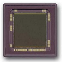
Page 42
... LUPA-4000 Data Sheet Figure 23: LUPA-4000 package specifications with die Cypress Semiconductor Corporation 3901 North First Street Contact: info@Fillfactory.com Document #: 38-05712 Rev.**(Revision 1.2 ) San Jose, CA 95134 408-943-2600 Page ...
Page 43
... LUPA-4000 Data Sheet 6.3 Bonding pads The bonding pads are located as indicated below. Figure 24: Placing of the bonding pads on the LUPA-4000 package Cypress Semiconductor Corporation Contact: info@Fillfactory.com Document #: 38-05712 Rev.**(Revision 1.2 ) 3901 North First Street San Jose, CA 95134 408-943-2600 Page ...
Page 44
... The die is bonded to the bonding pads of the package as indicated below. Figure 25: Bonding pads diagram of the LUPA-4000 package The die will be placed in the package in a way that the center of the light sensitive area will match the center of the package. Cypress Semiconductor Corporation Contact: info@Fillfactory.com Document #: 38-05712 Rev.**(Revision 1.2 ) ...
Page 45
... It is recommended that isopropyl alcohol (IPA) is used as a solvent for cleaning the image sensor glass lid. When using other solvents, it should be confirmed beforehand whether the solvent will dissolve the package and/or the glass lid or not. Cypress Semiconductor Corporation Contact: info@Fillfactory.com Document #: 38-05712 Rev.**(Revision 1.2 ) ...
Page 46
... FillFactory image sensors are only warranted to meet the specifications as described in the production data sheet. Specifications are subject to change without notice. Please contact info@FillFactory.com for more information. Cypress Semiconductor Corporation Contact: info@Fillfactory.com Document #: 38-05712 Rev.**(Revision 1.2 ) Cypress Semiconductor Part Number CYIL1SM4000AA-GBC 3901 North First Street San Jose, CA 95134 408-943-2600 Page ...
Page 47
... Default register values can be loaded to start the software in a desired state. Figure 26: Content of the LUPA-4000 evaluation kit Please contact Fillfactory (info@Fillfactory.com) if you want any more information on the evaluation kit. Cypress Semiconductor Corporation Contact: info@Fillfactory.com Document #: 38-05712 Rev.**(Revision 1.2 ) 3901 North First Street ...
Page 48
... It's important to notice that pixel signals above the double slope reset level will not be influenced by this double slope reset pulse (p1 and p2). Cypress Semiconductor Corporation Contact: info@Fillfactory.com Document #: 38-05712 Rev.**(Revision 1.2 ) ...
Page 49
... LUPA-4000 Data Sheet Document History Page Document Title: LUPA-4000 4M CMOS Image Sensor Document Number: 38-05712 Rev. ECN No. ** 310396 Cypress Semiconductor Corporation Contact: info@Fillfactory.com Document #: 38-05712 Rev.**(Revision 1.2 ) Issue Date Orig. of Change See ECN SIL (EOD) 3901 North First Street San Jose, CA 95134 ...