OM11048 NXP Semiconductors, OM11048 Datasheet - Page 10
OM11048
Manufacturer Part Number
OM11048
Description
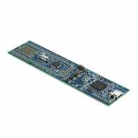
BOARD LPCXPRESSO LPC1343
Manufacturer
NXP Semiconductors
Series
LPCXpressor
Type
MCUr
Datasheet
1.OM11048.pdf
(62 pages)
Specifications of OM11048
Contents
Board, Software
Processor To Be Evaluated
LPC1343
Processor Series
LPC13xx
Interface Type
USB, I2C, UART
Maximum Operating Temperature
+ 85 C
Minimum Operating Temperature
- 40 C
Operating Supply Voltage
3.3 V
Tool Type
Demonstration Board
Core Architecture
ARM
Cpu Core
ARM Cortex M3
Data Bus Width
32 bit
Lead Free Status / RoHS Status
Lead free / RoHS Compliant
For Use With/related Products
LPC1343
Lead Free Status / Rohs Status
Lead free / RoHS Compliant
Other names
568-4947
Available stocks
Company
Part Number
Manufacturer
Quantity
Price

Part Number:
OM11048
Manufacturer:
NXP/恩智浦
Quantity:
20 000
Company:
Part Number:
OM11048Ј¬598
Manufacturer:
PH3
Quantity:
48


NXP Semiconductors
Table 3.
LPC1311_13_42_43
Product data sheet
Symbol
SWCLK/PIO0_10/
SCK/CT16B0_MAT2
R/PIO0_11/
AD0/CT32B0_MAT3
R/PIO1_0/
AD1/CT32B1_CAP0
R/PIO1_1/
AD2/CT32B1_MAT0
R/PIO1_2/
AD3/CT32B1_MAT1
SWDIO/PIO1_3/
AD4/
CT32B1_MAT2
PIO1_4/AD5/
CT32B1_MAT3/
WAKEUP
PIO1_5/RTS/
CT32B0_CAP0
PIO1_6/RXD/
CT32B0_MAT0
LPC1313/43 LQFP48 pin description table
Pin
29
32
33
34
35
39
40
45
46
[3]
[5]
[5]
[5]
[5]
[5]
[5]
[3]
[3]
Start
logic
input
yes
yes
yes
yes
yes
yes
yes
yes
yes
Type Reset
I
I/O
I/OO -
O
-
I/O
I
O
-
I/O
I
I
-
I/O
I
O
-
I/O
I
O
I/O
I/O
I
O
I/O
I
O
I
I/O
O
I
I/O
I
O
All information provided in this document is subject to legal disclaimers.
state
[1]
I; PU
-
-
I; PU
-
-
-
I; PU
-
-
-
I; PU
-
-
-
I; PU
-
-
-
I; PU
-
-
-
I; PU
-
-
-
I; PU
-
-
I; PU
-
-
Rev. 3 — 10 August 2010
Description
SWCLK — Serial wire clock.
PIO0_10 — General purpose digital input/output pin.
SCK — Serial clock for SSP.
CT16B0_MAT2 — Match output 2 for 16-bit timer 0.
R — Reserved. Configure for an alternate function in the IOCONFIG
block.
PIO0_11 — General purpose digital input/output pin.
AD0 — A/D converter, input 0.
CT32B0_MAT3 — Match output 3 for 32-bit timer 0.
R — Reserved. Configure for an alternate function in the IOCONFIG
block.
PIO1_0 — General purpose digital input/output pin.
AD1 — A/D converter, input 1.
CT32B1_CAP0 — Capture input 0 for 32-bit timer 1.
R — Reserved. Configure for an alternate function in the IOCONFIG
block.
PIO1_1 — General purpose digital input/output pin.
AD2 — A/D converter, input 2.
CT32B1_MAT0 — Match output 0 for 32-bit timer 1.
R — Reserved. Configure for an alternate function in the IOCONFIG
block.
PIO1_2 — General purpose digital input/output pin.
AD3 — A/D converter, input 3.
CT32B1_MAT1 — Match output 1 for 32-bit timer 1.
SWDIO — Serial wire debug input/output.
PIO1_3 — General purpose digital input/output pin.
AD4 — A/D converter, input 4.
CT32B1_MAT2 — Match output 2 for 32-bit timer 1.
PIO1_4 — General purpose digital input/output pin.
AD5 — A/D converter, input 5.
CT32B1_MAT3 — Match output 3 for 32-bit timer 1.
WAKEUP — Deep power-down mode wake-up pin. This pin must be
pulled HIGH externally to enter Deep power-down mode and pulled
LOW to exit Deep power-down mode.
PIO1_5 — General purpose digital input/output pin.
RTS — Request To Send output for UART.
CT32B0_CAP0 — Capture input 0 for 32-bit timer 0.
PIO1_6 — General purpose digital input/output pin.
RXD — Receiver input for UART.
CT32B0_MAT0 — Match output 0 for 32-bit timer 0.
…continued
32-bit ARM Cortex-M3 microcontroller
LPC1311/13/42/43
© NXP B.V. 2010. All rights reserved.
10 of 62
Related parts for OM11048
Image
Part Number
Description
Manufacturer
Datasheet
Request
R

Part Number:
Description:
NXP Semiconductors designed the LPC2420/2460 microcontroller around a 16-bit/32-bitARM7TDMI-S CPU core with real-time debug interfaces that include both JTAG andembedded trace
Manufacturer:
NXP Semiconductors
Datasheet:

Part Number:
Description:
NXP Semiconductors designed the LPC2458 microcontroller around a 16-bit/32-bitARM7TDMI-S CPU core with real-time debug interfaces that include both JTAG andembedded trace
Manufacturer:
NXP Semiconductors
Datasheet:
Part Number:
Description:
NXP Semiconductors designed the LPC2468 microcontroller around a 16-bit/32-bitARM7TDMI-S CPU core with real-time debug interfaces that include both JTAG andembedded trace
Manufacturer:
NXP Semiconductors
Datasheet:
Part Number:
Description:
NXP Semiconductors designed the LPC2470 microcontroller, powered by theARM7TDMI-S core, to be a highly integrated microcontroller for a wide range ofapplications that require advanced communications and high quality graphic displays
Manufacturer:
NXP Semiconductors
Datasheet:
Part Number:
Description:
NXP Semiconductors designed the LPC2478 microcontroller, powered by theARM7TDMI-S core, to be a highly integrated microcontroller for a wide range ofapplications that require advanced communications and high quality graphic displays
Manufacturer:
NXP Semiconductors
Datasheet:
Part Number:
Description:
The Philips Semiconductors XA (eXtended Architecture) family of 16-bit single-chip microcontrollers is powerful enough to easily handle the requirements of high performance embedded applications, yet inexpensive enough to compete in the market for hi
Manufacturer:
NXP Semiconductors
Datasheet:
Part Number:
Description:
The XA-S3 device is a member of Philips Semiconductors? XA(eXtended Architecture) family of high performance 16-bitsingle-chip microcontrollers
Manufacturer:
NXP Semiconductors
Datasheet:

Part Number:
Description:
The NXP BlueStreak LH75401/LH75411 family consists of two low-cost 16/32-bit System-on-Chip (SoC) devices
Manufacturer:
NXP Semiconductors
Datasheet:
Part Number:
Description:
The NXP LPC3130/3131 combine an 180 MHz ARM926EJ-S CPU core, high-speed USB2
Manufacturer:
NXP Semiconductors
Datasheet:
Part Number:
Description:
The NXP LPC3141 combine a 270 MHz ARM926EJ-S CPU core, High-speed USB 2
Manufacturer:
NXP Semiconductors
Part Number:
Description:
The NXP LPC3143 combine a 270 MHz ARM926EJ-S CPU core, High-speed USB 2
Manufacturer:
NXP Semiconductors

Part Number:
Description:
The NXP LPC3152 combines an 180 MHz ARM926EJ-S CPU core, High-speed USB 2
Manufacturer:
NXP Semiconductors
Part Number:
Description:
The NXP LPC3154 combines an 180 MHz ARM926EJ-S CPU core, High-speed USB 2
Manufacturer:
NXP Semiconductors

Part Number:
Description:
Standard level N-channel enhancement mode Field-Effect Transistor (FET) in a plastic package using NXP High-Performance Automotive (HPA) TrenchMOS technology
Manufacturer:
NXP Semiconductors
Datasheet: