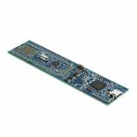
OM11048 NXP Semiconductors, OM11048 Datasheet - Page 26

OM11048
Manufacturer Part Number
OM11048
Description
BOARD LPCXPRESSO LPC1343
Manufacturer
NXP Semiconductors
Series
LPCXpressor
Type
MCUr
Datasheet
1.OM11048.pdf
(62 pages)
Specifications of OM11048
Contents
Board, Software
Processor To Be Evaluated
LPC1343
Processor Series
LPC13xx
Interface Type
USB, I2C, UART
Maximum Operating Temperature
+ 85 C
Minimum Operating Temperature
- 40 C
Operating Supply Voltage
3.3 V
Tool Type
Demonstration Board
Core Architecture
ARM
Cpu Core
ARM Cortex M3
Data Bus Width
32 bit
Lead Free Status / RoHS Status
Lead free / RoHS Compliant
For Use With/related Products
LPC1343
Lead Free Status / Rohs Status
Lead free / RoHS Compliant
Other names
568-4947
Available stocks
Company
Part Number
Manufacturer
Quantity
Price
Part Number:
OM11048
Manufacturer:
NXP/恩智浦
Quantity:
20 000
Company:
Part Number:
OM11048Ј¬598
Manufacturer:
PH3
Quantity:
48
NXP Semiconductors
LPC1311_13_42_43
Product data sheet
CAUTION
7.18.2 Reset
7.18.3 Brownout detection
7.18.4 Code security (Code Read Protection - CRP)
Reset has four sources on the LPC1311/13/42/43: the RESET pin, the Watchdog reset,
power-on reset (POR), and the Brown-Out Detection (BOD) circuit. The RESET pin is a
Schmitt trigger input pin. Assertion of chip reset by any source, once the operating voltage
attains a usable level, starts the IRC and initializes the flash controller.
When the internal reset is removed, the processor begins executing at address 0, which is
initially the reset vector mapped from the boot block. At that point, all of the processor and
peripheral registers have been initialized to predetermined values.
The LPC1311/13/42/43 includes four levels for monitoring the voltage on the V
this voltage falls below one of the four selected levels, the BOD asserts an interrupt signal
to the NVIC. This signal can be enabled for interrupt in the Interrupt Enable Register in the
NVIC in order to cause a CPU interrupt; if not, software can monitor the signal by reading
a dedicated status register. An additional threshold level can be selected to cause a
forced reset of the chip.
This feature of the LPC1311/13/42/43 allows user to enable different levels of security in
the system so that access to the on-chip flash and use of the Serial Wire Debugger (SWD)
and In-System Programming (ISP) can be restricted. When needed, CRP is invoked by
programming a specific pattern into a dedicated flash location. In-Application
Programming (IAP) commands are not affected by the CRP.
In addition, ISP entry via the PIO0_1 pin can be disabled without enabling CRP (NO_ISP
mode). For details see the LPC13xx user manual.
There are three levels of Code Read Protection:
1. CRP1 disables access to chip via the SWD and allows partial flash update (excluding
2. CRP2 disables access to chip via the SWD and only allows full flash erase and
3. Running an application with level CRP3 selected fully disables any access to chip via
flash sector 0) using a limited set of the ISP commands. This mode is useful when
CRP is required and flash field updates are needed but all sectors can not be erased.
update using a reduced set of the ISP commands.
the SWD pins and the ISP. This mode effectively disables ISP override using PIO0_1
pin, too. It is up to the user’s application to provide (if needed) flash update
mechanism using IAP calls or call reinvoke ISP command to enable flash update via
UART0.
If level three Code Read Protection (CRP3) is selected, no future factory testing can be
performed on the device.
All information provided in this document is subject to legal disclaimers.
Rev. 3 — 10 August 2010
32-bit ARM Cortex-M3 microcontroller
LPC1311/13/42/43
© NXP B.V. 2010. All rights reserved.
DD
pin. If
26 of 62


