AT91EB40A Atmel, AT91EB40A Datasheet - Page 17
AT91EB40A
Manufacturer Part Number
AT91EB40A
Description
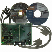
KIT EVAL FOR ARM AT91R40008
Manufacturer
Atmel
Series
AT91SAM Smart ARMr
Type
MCUr
Datasheet
1.AT91EB40A.pdf
(40 pages)
Specifications of AT91EB40A
Contents
Evaluation Board, Cable, Power Jack, CD-ROM
For Use With/related Products
AT91R40008
Lead Free Status / RoHS Status
Contains lead / RoHS non-compliant


4.1
4.2
4.2.1
4.2.2
4.3
AT91EB40A Evaluation Board User Guide
AT91R40008
Processor
Expansion
Connectors
I/O Expansion
Connector
EBI Expansion
Connector
Memories
Figure 6-1 in Section 6, “Appendix B – Schematics” shows the AT91R40008. The foot-
print is for a 100-pin TQFP package.
Jumper JP5A/JP5B (see Figure 6-7 in Section 6, “Appendix B – Schematics”) can be
removed by the user to allow measurement of the current on V
can be removed to measure the core microcontroller consumption on V
The two expansion connectors, I/O expansion connector and EBI expansion connector,
and the JTAG interface are described below.
The I/O and EBI expansion connectors’ pinout and position are compatible with other
AT91 evaluation boards (except the I/O expansion connector pinout and position of the
EB40) so that users can connect their prototype daughter boards to any of these evalu-
ation boards.
The I/O expansion connector P2 makes the general-purpose I/O (GPIO) lines, VCC3V3
and Ground, available to the user. Configuration straps are used to select between the
I/O lines being used by the evaluation board or by the user via the I/O expansion con-
nector. The connector fitted at the factory is a 32 x 2 connector on a 0.1” (2.54 mm)
pitch.
The EBI expansion connector P1 makes the data bus, address bus, chip select,
read/write signals, oscillator output, wait request pins, VCC3V3 and Ground available to
the user. The connector fitted at the factory is a 32 x 2 connector on a 0.1” (2.54 mm)
pitch.
The schematic (Figure 6-2 on page 6-3 in Section 6, “Appendix B – Schematics”) shows
two 128K/512K x 8 SRAM devices that can be added to the AT91EB40A.
Note:
Figure 6-8 on page 6-9 shows the Flash memories. The printed circuit board of the
EB40A provides two footprints (U1A and U1B) for two different Flash memories. At fac-
tory, the EB40A fits an AT49BV162A Flash memory (U1A). U1A footprint can also
accept an AT49BV161 Flash memory. An extra Flash memory can be added on U1B
footprint. The U1B footprint can accept an AT49BV8011 or an AT49BV400 Flash mem-
ory. The Flash memory on U1A and the Flash memory on U1B cannot be used at the
The AT91EB40A evaluation board does not feature any external SRAM. The
user can add SRAM ranging in size from 256K bytes x 16 bits to 1M byte x 16
bits. See “Increasing Memory Size” on page 5-4 for SRAM references.
Circuit Description
DDIO
Rev. 2635C–ATARM–13-May-05
Section 4
. Jumper JP7A/JP7B
DDCORE
.
4-1
Related parts for AT91EB40A
Image
Part Number
Description
Manufacturer
Datasheet
Request
R

Part Number:
Description:
DEV KIT FOR AVR/AVR32
Manufacturer:
Atmel
Datasheet:

Part Number:
Description:
INTERVAL AND WIPE/WASH WIPER CONTROL IC WITH DELAY
Manufacturer:
ATMEL Corporation
Datasheet:
Part Number:
Description:
Low-Voltage Voice-Switched IC for Hands-Free Operation
Manufacturer:
ATMEL Corporation
Datasheet:
Part Number:
Description:
MONOLITHIC INTEGRATED FEATUREPHONE CIRCUIT
Manufacturer:
ATMEL Corporation
Datasheet:
Part Number:
Description:
AM-FM Receiver IC U4255BM-M
Manufacturer:
ATMEL Corporation
Datasheet:
Part Number:
Description:
Monolithic Integrated Feature Phone Circuit
Manufacturer:
ATMEL Corporation
Datasheet:
Part Number:
Description:
Multistandard Video-IF and Quasi Parallel Sound Processing
Manufacturer:
ATMEL Corporation
Datasheet:
Part Number:
Description:
High-performance EE PLD
Manufacturer:
ATMEL Corporation
Datasheet:
Part Number:
Description:
8-bit Flash Microcontroller
Manufacturer:
ATMEL Corporation
Datasheet:
Part Number:
Description:
2-Wire Serial EEPROM
Manufacturer:
ATMEL Corporation
Datasheet: