EVAL-ADUC847QSZ Analog Devices Inc, EVAL-ADUC847QSZ Datasheet - Page 36
EVAL-ADUC847QSZ
Manufacturer Part Number
EVAL-ADUC847QSZ
Description
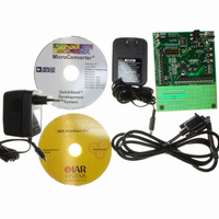
KIT DEV QUICK START FOR ADUC847
Manufacturer
Analog Devices Inc
Series
QuickStart™ Kitr
Type
MCUr
Datasheet
1.EVAL-ADUC845QSZ.pdf
(108 pages)
Specifications of EVAL-ADUC847QSZ
Contents
Evaluation Board, Power Supply, Cable, Software and Documentation
Silicon Manufacturer
Analog Devices
Core Architecture
8051
Silicon Core Number
ADuC847
Tool / Board Applications
General Purpose MCU, MPU, DSP, DSC
Mcu Supported Families
ADUC8xx
Development Tool Type
Hardware - Eval/Demo Board
Rohs Compliant
Yes
Lead Free Status / RoHS Status
Lead free / RoHS Compliant
For Use With/related Products
ADuC847
Lead Free Status / RoHS Status
Lead free / RoHS Compliant, Lead free / RoHS Compliant


ADuC845/ADuC847/ADuC848
DATA OUTPUT CODING
When the primary ADC is configured for unipolar operation,
the output coding is natural (straight) binary with a zero differ-
ential input voltage resulting in a code of 000...000, a midscale
voltage resulting in a code of 100...000, and a full-scale voltage
resulting in a code of 111...111. The output code for any analog
input voltage on the main ADC can be represented as follows:
where:
AIN is the analog input voltage.
GAIN is the PGA gain setting, that is, 1 on the 2.56 V range and
128 on the 20 mV range, and N = 24 (16 on the ADuC848).
The output code for any analog input voltage on the auxiliary
ADC can
with the same definitions as used for the primary ADC above.
When the primary ADC is conf ured for bipolar operation, the
coding is offset binary with negative full-scale voltage resulting
in a code of 000...000, a zero differential voltage resulting in a
code of 800…000, and a positive full-scale voltage resulting in a
code of 111...111. The output from the primary ADC for any
analog input voltage can be represented as follows:
where:
AIN is the analog input voltage.
GAIN is the PGA gain, that is, 1 on the ±2.56 V range and
128 on the ±20 mV range.
N = 24 (16 on the ADuC848).
The output from the auxiliary ADC in bipolar mode can be
represented as follows:
Code – (AIN × GAIN × 2
Code = (AIN × 2
Code = 2
Code = 2
be represented as follows:
N−1
N−1
[(AIN × GAIN)/(1.024 ×V
[(AIN/V
N
)/(V
REF
REF
) + 1]
)
N
)/(1.024 × V
ig
REF
REF
) + 1]
)
Rev. B | Page 36 of 108
EXCITATION CURRENTS
The ADuC845/ADuC847/ADuC848 contain two matched,
software-configurable 200 µA current sources. Both source
current from AV
IEXC1 (Pin 11 whose alternate functions are P1.6/AIN7) or
IEXC2 (Pin 12, whose alternate functions are P1.7/AIN8) pins
on the device. These currents are controlled via the lower four
bits in the ICON register (Table 30). These bits not only enable
the current sources but also allow the configuration of the
currents such that 200 µA can be sourced individually from
both pins or can be combined to give a 400 µA source from one
or the other of the outputs. These sources can be used to excite
external resistive bridge or RTD sensors (see Figure 71).
ADC POWER-ON
The ADC typically takes 0.5 ms to power up from an initial
start-up seque
nce or following a power-down event.
DD
, which is directed to either or both of the
Related parts for EVAL-ADUC847QSZ
Image
Part Number
Description
Manufacturer
Datasheet
Request
R


Part Number:
Description:
BOARD EVAL FOR SI270X-A
Manufacturer:
Silicon Laboratories Inc
Datasheet:

Part Number:
Description:
BUCK CONV REF DESIGN KIT IP1201
Manufacturer:
International Rectifier
Datasheet:
Part Number:
Description:
BOARD DEMO SYNC DUAL BUCK CNVTER
Manufacturer:
International Rectifier
Datasheet:
Part Number:
Description:
BOARD DEMO SYNC BUCK CONVETER
Manufacturer:
International Rectifier
Datasheet:

Part Number:
Description:
EVALBOARD/EB Omnidirectional microphone - Analog
Manufacturer:
Analog Devices
Datasheet:
Part Number:
Description:
EVALBOARD/EB Omnidirectional microphone - Analog
Manufacturer:
Analog Devices
Datasheet:


Part Number:
Description:
BOARD EVAL LED DRIVER LT3756
Manufacturer:
Linear Technology
Datasheet:

Part Number:
Description:
BOARD EVAL FOR AD7741/7742
Manufacturer:
Analog Devices Inc
Datasheet:

Part Number:
Description:
±1.7g Dual-Axis IMEMS Accelerometer Evaluation Board
Manufacturer:
Analog Devices Inc
Datasheet:

Part Number:
Description:
IC MULTIPLIER ANALOG 8-SOIC T/R
Manufacturer:
Analog Devices Inc
Datasheet:

Part Number:
Description:
IC ANALOG MULTIPLIER 8-DIP
Manufacturer:
Analog Devices Inc
Datasheet:
Part Number:
Description:
IC ANALOG MULTIPLIER 8-SOIC
Manufacturer:
Analog Devices Inc
Datasheet:
Part Number:
Description:
IC ANALOG MULTIPLIER 8-DIP
Manufacturer:
Analog Devices Inc
Datasheet: