EVAL-ADUC847QSZ Analog Devices Inc, EVAL-ADUC847QSZ Datasheet - Page 4
EVAL-ADUC847QSZ
Manufacturer Part Number
EVAL-ADUC847QSZ
Description
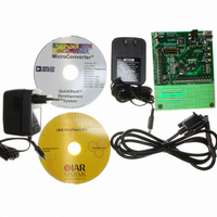
KIT DEV QUICK START FOR ADUC847
Manufacturer
Analog Devices Inc
Series
QuickStart™ Kitr
Type
MCUr
Datasheet
1.EVAL-ADUC845QSZ.pdf
(108 pages)
Specifications of EVAL-ADUC847QSZ
Contents
Evaluation Board, Power Supply, Cable, Software and Documentation
Silicon Manufacturer
Analog Devices
Core Architecture
8051
Silicon Core Number
ADuC847
Tool / Board Applications
General Purpose MCU, MPU, DSP, DSC
Mcu Supported Families
ADUC8xx
Development Tool Type
Hardware - Eval/Demo Board
Rohs Compliant
Yes
Lead Free Status / RoHS Status
Lead free / RoHS Compliant
For Use With/related Products
ADuC847
Lead Free Status / RoHS Status
Lead free / RoHS Compliant, Lead free / RoHS Compliant


ADuC845/ADuC847/ADuC848
SPECIFICATIONS
AV
DGND = 0 V; XTAL1/XTAL2 = 32.768 kHz crystal; all specifications T
ADC, unless otherwise noted. Core speed = 1.57 MHz (default CD = 3), unless otherwise noted.
Table 1.
Parameter
PRIMARY ADC
PRIMARY ADC ANALOG INPUTS
Footnotes at end of table.
Conversion Rate
No Missing Codes
Resolution (ADuC845/ADuC847)
Resolution (ADuC848)
Output Noise (ADuC845/ADuC847)
Output Noise (ADuC848)
Integral Nonlinearity
Offset Error
Offset Error Drift vs. Temperature
Full-Scale Error
Gain Error Drift vs. Temperature
Power Supply Rejection
Differential Input Voltage Ranges
Bipolar Mode (ADC0CON1.5 = 0)
Unipolar Mode (ADC0CON1.5 = 1)
ADC Range Matching
Common-Mode Rejection DC
Common-Mode Rejection
50 Hz/60 Hz
DD
ADuC845/ADuC847
ADuC848
On AIN
On AIN
= 2.7 V to 3.6 V or 4.75 V to 5.25 V, DV
3
2
4
2
1
4
, 5 6
2
Min
16.06
24
24
See Table 11 and Table 15
See Table 13 and Table 17
See Table 10 and Table 14
See Table 12 and Table 16
80
95
95
90
5.4
DD
= 2.7 V to 3.6 V or 4.75 V to 5.25 V, REFIN(+) = 2.5 V, REFIN(–) = AGND; AGND =
Typ
±3
±10
±200
±10
±10
±0.5
±0.5
113
80
±1.024 ×
V
0 – 1.024 ×
V
±2
113
REF
REF
/GAIN
/GAIN
Rev. B | Page 4 of 108
Max
105
1365
±15
MIN
to T
Unit
Hz
Hz
Bits
Bits
µV (rms)
µV (rms)
ppm of FSR
µV
nV/°C
nV/°C
µV
µV
LSB
ppm/°C
dB
dB
dB
V
V
µV
dB
dB
dB
dB
MAX
16
, unless otherwise noted. Input buffer on for primary
Conditions
Chop on (ADCMODE.3 = 0)
Chop off (ADCMODE.3 = 1)
≤26.7 Hz update rate with chop enabled
≤80.3 Hz update rate with chop disabled
Output noise varies with selected update rates,
Output noise varies with selected update rates,
1 LSB
Chop on
Chop off, offset error is in the order of the noise
Chop on (ADCMODE.3 = 0)
Chop off (ADCMODE.3 = 1)
±20 mV to ±2.56 V
±20 mV to ±640 mV
±1.28 V to ±2.56 V
AIN = 1 V, ±2.56 V, chop enabled
AIN = 7.8 mV, ±20 mV, chop enabled
AIN = 1 V, ±2.56 V, chop disabled
Gain = 1 to 128
V
V
AIN = 18 mV, chop enabled
Chop enabled, chop disabled
AIN = 7.8 mV, range = ±20 mV
AIN = 1 V, range = ±2.56 V
50 Hz/60 Hz ± 1 Hz, 16.6 Hz and 50 Hz update
AIN = 7.8 mV, range = ±20 mV
AIN = 1 V, range = ±2.56 V
REF
REF
gain range, and chop status.
gain range, and chop status.
for the programmed gain and update rate
following a calibration.
REFIN2(+) − REFIN2(−) (or Int 1.25 V
REFIN2(+) − REFIN2(−) (or Int 1.25 V
rate, chop enabled, REJ60 enabled
= REFIN(+) − REFIN(−) or
= REFIN(+) − REFIN(−) or
16
2
REF
REF
)
)
Related parts for EVAL-ADUC847QSZ
Image
Part Number
Description
Manufacturer
Datasheet
Request
R


Part Number:
Description:
BOARD EVAL FOR SI270X-A
Manufacturer:
Silicon Laboratories Inc
Datasheet:

Part Number:
Description:
BUCK CONV REF DESIGN KIT IP1201
Manufacturer:
International Rectifier
Datasheet:
Part Number:
Description:
BOARD DEMO SYNC DUAL BUCK CNVTER
Manufacturer:
International Rectifier
Datasheet:
Part Number:
Description:
BOARD DEMO SYNC BUCK CONVETER
Manufacturer:
International Rectifier
Datasheet:

Part Number:
Description:
EVALBOARD/EB Omnidirectional microphone - Analog
Manufacturer:
Analog Devices
Datasheet:
Part Number:
Description:
EVALBOARD/EB Omnidirectional microphone - Analog
Manufacturer:
Analog Devices
Datasheet:


Part Number:
Description:
BOARD EVAL LED DRIVER LT3756
Manufacturer:
Linear Technology
Datasheet:

Part Number:
Description:
BOARD EVAL FOR AD7741/7742
Manufacturer:
Analog Devices Inc
Datasheet:

Part Number:
Description:
±1.7g Dual-Axis IMEMS Accelerometer Evaluation Board
Manufacturer:
Analog Devices Inc
Datasheet:

Part Number:
Description:
IC MULTIPLIER ANALOG 8-SOIC T/R
Manufacturer:
Analog Devices Inc
Datasheet:

Part Number:
Description:
IC ANALOG MULTIPLIER 8-DIP
Manufacturer:
Analog Devices Inc
Datasheet:
Part Number:
Description:
IC ANALOG MULTIPLIER 8-SOIC
Manufacturer:
Analog Devices Inc
Datasheet:
Part Number:
Description:
IC ANALOG MULTIPLIER 8-DIP
Manufacturer:
Analog Devices Inc
Datasheet: