EVAL-ADUC847QSZ Analog Devices Inc, EVAL-ADUC847QSZ Datasheet - Page 53
EVAL-ADUC847QSZ
Manufacturer Part Number
EVAL-ADUC847QSZ
Description
KIT DEV QUICK START FOR ADUC847
Manufacturer
Analog Devices Inc
Series
QuickStart™ Kitr
Type
MCUr
Datasheet
1.EVAL-ADUC845QSZ.pdf
(108 pages)
Specifications of EVAL-ADUC847QSZ
Contents
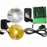
Evaluation Board, Power Supply, Cable, Software and Documentation
Silicon Manufacturer
Analog Devices
Core Architecture
8051
Silicon Core Number
ADuC847
Tool / Board Applications
General Purpose MCU, MPU, DSP, DSC
Mcu Supported Families
ADUC8xx
Development Tool Type
Hardware - Eval/Demo Board
Rohs Compliant
Yes
Lead Free Status / RoHS Status
Lead free / RoHS Compliant
For Use With/related Products
ADuC847
Lead Free Status / RoHS Status
Lead free / RoHS Compliant, Lead free / RoHS Compliant


DAC CIRCUIT INFORMATION
The ADuC845/ADuC847/ADuC848 incorporate a 12-bit,
voltage output DAC on-chip. It has a rail-to-rail voltage output
buffer capable of driving 10 kΩ/100 pF, and has two selectable
ranges, 0 V to V
8-bit mode. The DAC has a control register, DACCON, and two
data registers, DACH/L. The DAC output can be programmed
to appear at Pin 14 (DAC) or Pin 13 (AINCOM).
DACCON Control Register
SFR Address:
Power-On Default:
Bit Addressable:
Table 33. DACCON—DAC Configuration Commands
Bit No.
7
6
5
4
3
2
1
0
DACH/DACL Data Registers
These DAC data registers are written to by the user to update
the DAC output.
SFR Address:
Power-On Default:
Bit Addressable:
Name
–––
–––
–––
DACPIN
DAC8
DACRN
DACCLR
DACEN
REF
and 0 V to AV
FDH
00H
No
DACH (DAC data high byte)—FCH
00H (both registers)
No (both registers)
DACL (DAC data low byte)—FBH
DAC Output Pin Select.
DAC Clear Bit.
DAC Enable Bit.
Description
Not Implemented. Write Don’t Care.
Not Implemented. Write Don’t Care.
Not Implemented. Write Don’t Care.
Set to 1 by the user to direct the DAC output to Pin 13 (AINCOM).
Cleared to 0 by the user to direct the DAC output to Pin 14 (DAC).
DAC 8-Bit Mode Bit.
Set to 1 by the user to enable 8-bit DAC operation. In this mode, the 8 bits in DACL SFR are routed to the 8 MSBs
of the DAC, and the 4 LSBs of the DAC are set to 0.
Cleared to 0 by the user to enable 12-bit DAC operation. In this mode, the 8 LSBs of the result are routed to
DACL, and the upper 4 MSB bits are routed to the lower 4 bits of DACH.
DAC Output Range Bit.
Set to 1 by the user to configure the DAC range of 0 V to AV
Cleared to 0 by the user to configure the DAC range of 0 V to 2.5 V (V
Set to 1 by the user to enable normal DAC operation.
Cleared to 0 by the user to reset the DAC data registers DACL/H to 0.
Set to 1 by the user to enable normal DAC operation.
Cleared to 0 by the user to power down the DAC.
DD
. It can operate in 12-bit or
Rev. B | Page 53 of 108
In 12-bit mode, the DAC voltage output is updated as soon as
the DACL data SFR is written; therefore, the DAC data registers
should be updated as DACH first, followed by DACL. The 12-
bit DAC data should be written into DACH/L right-justified
such that DACL contains the lower 8 bits, and the lower nibble
of DACH contains the upper 4 bits.
DD
.
ADuC845/ADuC847/ADuC848
REF
).
Related parts for EVAL-ADUC847QSZ
Image
Part Number
Description
Manufacturer
Datasheet
Request
R


Part Number:
Description:
BOARD EVAL FOR SI270X-A
Manufacturer:
Silicon Laboratories Inc
Datasheet:

Part Number:
Description:
BUCK CONV REF DESIGN KIT IP1201
Manufacturer:
International Rectifier
Datasheet:
Part Number:
Description:
BOARD DEMO SYNC DUAL BUCK CNVTER
Manufacturer:
International Rectifier
Datasheet:
Part Number:
Description:
BOARD DEMO SYNC BUCK CONVETER
Manufacturer:
International Rectifier
Datasheet:

Part Number:
Description:
EVALBOARD/EB Omnidirectional microphone - Analog
Manufacturer:
Analog Devices
Datasheet:
Part Number:
Description:
EVALBOARD/EB Omnidirectional microphone - Analog
Manufacturer:
Analog Devices
Datasheet:


Part Number:
Description:
BOARD EVAL LED DRIVER LT3756
Manufacturer:
Linear Technology
Datasheet:

Part Number:
Description:
BOARD EVAL FOR AD7741/7742
Manufacturer:
Analog Devices Inc
Datasheet:

Part Number:
Description:
±1.7g Dual-Axis IMEMS Accelerometer Evaluation Board
Manufacturer:
Analog Devices Inc
Datasheet:

Part Number:
Description:
IC MULTIPLIER ANALOG 8-SOIC T/R
Manufacturer:
Analog Devices Inc
Datasheet:

Part Number:
Description:
IC ANALOG MULTIPLIER 8-DIP
Manufacturer:
Analog Devices Inc
Datasheet:
Part Number:
Description:
IC ANALOG MULTIPLIER 8-SOIC
Manufacturer:
Analog Devices Inc
Datasheet:
Part Number:
Description:
IC ANALOG MULTIPLIER 8-DIP
Manufacturer:
Analog Devices Inc
Datasheet: