C8051F336DK Silicon Laboratories Inc, C8051F336DK Datasheet - Page 5
C8051F336DK
Manufacturer Part Number
C8051F336DK
Description
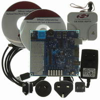
DEV KIT FOR C8051F336
Manufacturer
Silicon Laboratories Inc
Type
MCUr
Specifications of C8051F336DK
Contents
Evaluation Board, Power Supply, USB Cables, Adapter and Documentation
Processor To Be Evaluated
C8051F33x
Interface Type
USB, UART
Operating Supply Voltage
7 V to 15 V
Lead Free Status / RoHS Status
Lead free / RoHS Compliant
For Use With/related Products
C8051F336
Lead Free Status / Rohs Status
Lead free / RoHS Compliant
Other names
336-1430


21. SMBus................................................................................................................... 138
22. UART0 ................................................................................................................... 159
23. Enhanced Serial Peripheral Interface (SPI0) ..................................................... 167
20.2. Assigning Port I/O Pins to Analog and Digital Functions............................... 122
20.3. Priority Crossbar Decoder ............................................................................. 124
20.4. Port I/O Initialization ...................................................................................... 126
20.5. Port Match ..................................................................................................... 129
20.6. Special Function Registers for Accessing and Configuring Port I/O ............. 131
21.1. Supporting Documents .................................................................................. 139
21.2. SMBus Configuration..................................................................................... 139
21.3. SMBus Operation .......................................................................................... 139
21.4. Using the SMBus........................................................................................... 141
21.5. SMBus Transfer Modes................................................................................. 151
21.6. SMBus Status Decoding................................................................................ 154
22.1. Enhanced Baud Rate Generation.................................................................. 160
22.2. Operational Modes ........................................................................................ 161
22.3. Multiprocessor Communications ................................................................... 163
23.1. Signal Descriptions........................................................................................ 168
23.2. SPI0 Master Mode Operation ........................................................................ 169
23.3. SPI0 Slave Mode Operation .......................................................................... 170
20.1.3. Interfacing Port I/O to 5V Logic ............................................................. 121
20.2.1. Assigning Port I/O Pins to Analog Functions ........................................ 122
20.2.2. Assigning Port I/O Pins to Digital Functions.......................................... 122
20.2.3. Assigning Port I/O Pins to External Event Trigger Functions................ 123
21.3.1. Transmitter Vs. Receiver....................................................................... 140
21.3.2. Arbitration.............................................................................................. 140
21.3.3. Clock Low Extension............................................................................. 140
21.3.4. SCL Low Timeout.................................................................................. 140
21.3.5. SCL High (SMBus Free) Timeout ......................................................... 141
21.4.1. SMBus Configuration Register.............................................................. 141
21.4.2. SMB0CN Control Register .................................................................... 145
21.4.3. Hardware Slave Address Recognition .................................................. 147
21.4.4. Data Register ........................................................................................ 150
21.5.1. Write Sequence (Master) ...................................................................... 151
21.5.2. Read Sequence (Master) ...................................................................... 152
21.5.3. Write Sequence (Slave) ........................................................................ 153
21.5.4. Read Sequence (Slave) ........................................................................ 154
22.2.1. 8-Bit UART ............................................................................................ 161
22.2.2. 9-Bit UART ............................................................................................ 162
23.1.1. Master Out, Slave In (MOSI)................................................................. 168
23.1.2. Master In, Slave Out (MISO)................................................................. 168
23.1.3. Serial Clock (SCK) ................................................................................ 168
23.1.4. Slave Select (NSS) ............................................................................... 168
21.4.2.1. Software ACK Generation ............................................................ 145
21.4.2.2. Hardware ACK Generation ........................................................... 145
Rev.1.0
C8051F336/7/8/9
5
Related parts for C8051F336DK
Image
Part Number
Description
Manufacturer
Datasheet
Request
R

Part Number:
Description:
SMD/C°/SINGLE-ENDED OUTPUT SILICON OSCILLATOR
Manufacturer:
Silicon Laboratories Inc
Part Number:
Description:
Manufacturer:
Silicon Laboratories Inc
Datasheet:
Part Number:
Description:
N/A N/A/SI4010 AES KEYFOB DEMO WITH LCD RX
Manufacturer:
Silicon Laboratories Inc
Datasheet:
Part Number:
Description:
N/A N/A/SI4010 SIMPLIFIED KEY FOB DEMO WITH LED RX
Manufacturer:
Silicon Laboratories Inc
Datasheet:
Part Number:
Description:
N/A/-40 TO 85 OC/EZLINK MODULE; F930/4432 HIGH BAND (REV E/B1)
Manufacturer:
Silicon Laboratories Inc
Part Number:
Description:
EZLink Module; F930/4432 Low Band (rev e/B1)
Manufacturer:
Silicon Laboratories Inc
Part Number:
Description:
I°/4460 10 DBM RADIO TEST CARD 434 MHZ
Manufacturer:
Silicon Laboratories Inc
Part Number:
Description:
I°/4461 14 DBM RADIO TEST CARD 868 MHZ
Manufacturer:
Silicon Laboratories Inc
Part Number:
Description:
I°/4463 20 DBM RFSWITCH RADIO TEST CARD 460 MHZ
Manufacturer:
Silicon Laboratories Inc
Part Number:
Description:
I°/4463 20 DBM RADIO TEST CARD 868 MHZ
Manufacturer:
Silicon Laboratories Inc
Part Number:
Description:
I°/4463 27 DBM RADIO TEST CARD 868 MHZ
Manufacturer:
Silicon Laboratories Inc
Part Number:
Description:
I°/4463 SKYWORKS 30 DBM RADIO TEST CARD 915 MHZ
Manufacturer:
Silicon Laboratories Inc
Part Number:
Description:
N/A N/A/-40 TO 85 OC/4463 RFMD 30 DBM RADIO TEST CARD 915 MHZ
Manufacturer:
Silicon Laboratories Inc
Part Number:
Description:
I°/4463 20 DBM RADIO TEST CARD 169 MHZ
Manufacturer:
Silicon Laboratories Inc