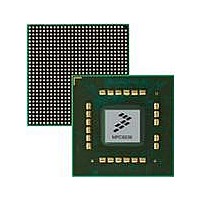
MPC8536DS Freescale Semiconductor, MPC8536DS Datasheet - Page 115

MPC8536DS
Manufacturer Part Number
MPC8536DS
Description
BOARD DEV SYSTEM MPC8536E
Manufacturer
Freescale Semiconductor
Series
PowerQUICC III™r
Type
MPUr
Datasheets
1.MPC8536EBVTAVLA.pdf
(127 pages)
2.MPC8536EBVTAVLA.pdf
(1706 pages)
3.MPC8536DS.pdf
(2 pages)
4.MPC8536DS.pdf
(126 pages)
Specifications of MPC8536DS
Contents
Board, Software and Documentation
Processor Series
MPC85xx
Core
e500
Data Bus Width
32 bit
Maximum Clock Frequency
667 MHz
Operating Supply Voltage
- 0.3 V to + 1.21 V
Maximum Operating Temperature
+ 105 C
Data Ram Size
32 KB
Interface Type
SPI, USB
Program Memory Type
DDR2, DDR3, SDRAM
Core Size
32 Bit
Program Memory Size
544KB
Cpu Speed
1.5GHz
Digital Ic Case Style
BGA
No. Of Pins
783
Supply Voltage Range
0.95V To 1.05V
Rohs Compliant
Yes
For Use With/related Products
MPC8536
Lead Free Status / RoHS Status
Lead free / RoHS Compliant
This figure shows the PLL power supply filter circuit.
The AV
the power supplied to the PLL is filtered using a circuit similar to the one shown in following
effectiveness, the filter circuit is placed as closely as possible to the AV
as possible. The ground connection should be near the AV
followed by the 1-µF capacitor, and finally the 1 ohm resistor to the board supply plane. The capacitors are connected from
AV
should be kept short, wide and direct.
Note the following:
3.3
In all low power mode by default, all input and output pads remain driven as per normal functional operation. The inputs remain
enabled.
The exception is that in Deep Sleep mode, GCR[DEEPSLEEP_Z] can be used to tristate a subset of output pads, and disable
the receivers of input pads as defined in
for details.
3.4
Due to large address and data buses, and high operating frequencies, this chip can generate transient power surges and high
frequency noise in its power supply, especially while driving large capacitive loads. This noise must be prevented from reaching
other components in the chip system, and the chip itself requires a clean, tightly regulated source of power. Therefore, it is
recommended that the system designer place at least one decoupling capacitor at each V
LV
and LV
be placed directly under the chip using a standard escape pattern as much as possible. If some caps are to be placed surrounding
the part it should be routed with short and large trace to minimize the inductance.
Freescale Semiconductor
DD
DD
•
•
_SRDSn to the ground plane. Use ceramic chip capacitors with the highest possible self-resonant frequency. All traces
pin of the chip. These decoupling capacitors should receive their power from separate V
DD
DD
AV
Signals on the SerDes interface are fed from the XV
, and GND power planes in the PCB, utilizing short low impedance traces to minimize inductance. Capacitors must
_SRDSn signals provides power for the analog portions of the SerDes PLL. To ensure stability of the internal clock,
Pin States in Deep Sleep State
Decoupling Recommendations
DD
should be a filtered version of SV
MPC8536E PowerQUICC III Integrated Processor Hardware Specifications, Rev. 4
SnV
V
DD
DD
1. An 0805 sized capacitor is recommended for system initial bring-up
Figure 76. SerDes PLL Power Supply Filter Circuit
Figure 75. Chip PLL Power Supply Filter Circuit
10 Ω
1.0 Ω
Table
1. See the MPC8536E PowerQUICC III Integrated Processor Reference Manual
2.2 µF
DD
2.2 µF
.
DD
1
GND
_SRDSn balls. The 0.003-µF capacitor is closest to the balls,
DD
GND
power plane.
Low ESL Surface Mount Capacitors
2.2 µF
2.2 µF
DD
_SRDSn balls to ensure it filters out as much noise
1
AV
0.003 µF
DD
DD
, TV
Hardware Design Considerations
DD,
AV
Figure
DD
TV
DD -
, BV
DD
SRDS
76. For maximum
DD
, BV
, OV
DD
, OV
DD
, GV
DD
, GV
DD
, and
DD
115
,


