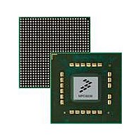
MPC8536DS Freescale Semiconductor, MPC8536DS Datasheet - Page 79

MPC8536DS
Manufacturer Part Number
MPC8536DS
Description
BOARD DEV SYSTEM MPC8536E
Manufacturer
Freescale Semiconductor
Series
PowerQUICC III™r
Type
MPUr
Datasheets
1.MPC8536EBVTAVLA.pdf
(127 pages)
2.MPC8536EBVTAVLA.pdf
(1706 pages)
3.MPC8536DS.pdf
(2 pages)
4.MPC8536DS.pdf
(126 pages)
Specifications of MPC8536DS
Contents
Board, Software and Documentation
Processor Series
MPC85xx
Core
e500
Data Bus Width
32 bit
Maximum Clock Frequency
667 MHz
Operating Supply Voltage
- 0.3 V to + 1.21 V
Maximum Operating Temperature
+ 105 C
Data Ram Size
32 KB
Interface Type
SPI, USB
Program Memory Type
DDR2, DDR3, SDRAM
Core Size
32 Bit
Program Memory Size
544KB
Cpu Speed
1.5GHz
Digital Ic Case Style
BGA
No. Of Pins
783
Supply Voltage Range
0.95V To 1.05V
Rohs Compliant
Yes
For Use With/related Products
MPC8536
Lead Free Status / RoHS Status
Lead free / RoHS Compliant
- MPC8536EBVTAVLA PDF datasheet
- MPC8536EBVTAVLA PDF datasheet #2
- MPC8536DS PDF datasheet #3
- MPC8536DS PDF datasheet #4
- Current page: 79 of 126
- Download datasheet (2Mb)
This figure provides the AC test load for TDO and the boundary-scan outputs.
This figure provides the JTAG clock input timing diagram.
This figure provides the TRST timing diagram.
This figure provides the boundary-scan timing diagram.
2.16
This section describes the DC and AC electrical specifications for the serial ATA (SATA) of the chip. Note that the external
cabled applications or long backplane applications (Gen1x & Gen2x) are not supported.
Freescale Semiconductor
Serial ATA (SATA)
External Clock
Data Outputs
Data Inputs
External Clock
Boundary
Boundary
MPC8536E PowerQUICC III Integrated Processor Hardware Specifications, Rev. 4
TRST
JTAG
JTAG
Output
t
JTKLDX
Figure 45. AC Test Load for the JTAG Interface
Figure 46. JTAG Clock Input Timing Diagram
Figure 48. Boundary-Scan Timing Diagram
VM
t
JTKHKL
VM = Midpoint Voltage (OV DD /2)
Figure 47. TRST Timing Diagram
VM
Z
VM
VM = Midpoint Voltage (OV DD /2)
VM = Midpoint Voltage (OV DD /2)
t
0
JTKLDV
t
= 50 Ω
JTG
VM
t
TRST
t
JTDVKH
VM
R
VM
Output Data Valid
L
Data Valid
= 50 Ω
Input
t
JTGR
VM
OV
DD
t
t
JTDXKH
JTGF
/2
Electrical Characteristics
79
Related parts for MPC8536DS
Image
Part Number
Description
Manufacturer
Datasheet
Request
R
Part Number:
Description:
Manufacturer:
Freescale Semiconductor, Inc
Datasheet:
Part Number:
Description:
Manufacturer:
Freescale Semiconductor, Inc
Datasheet:
Part Number:
Description:
Manufacturer:
Freescale Semiconductor, Inc
Datasheet:
Part Number:
Description:
Manufacturer:
Freescale Semiconductor, Inc
Datasheet:
Part Number:
Description:
Manufacturer:
Freescale Semiconductor, Inc
Datasheet:
Part Number:
Description:
Manufacturer:
Freescale Semiconductor, Inc
Datasheet:
Part Number:
Description:
Manufacturer:
Freescale Semiconductor, Inc
Datasheet:
Part Number:
Description:
Manufacturer:
Freescale Semiconductor, Inc
Datasheet:
Part Number:
Description:
Manufacturer:
Freescale Semiconductor, Inc
Datasheet:
Part Number:
Description:
Manufacturer:
Freescale Semiconductor, Inc
Datasheet:
Part Number:
Description:
Manufacturer:
Freescale Semiconductor, Inc
Datasheet:
Part Number:
Description:
Manufacturer:
Freescale Semiconductor, Inc
Datasheet:
Part Number:
Description:
Manufacturer:
Freescale Semiconductor, Inc
Datasheet:
Part Number:
Description:
Manufacturer:
Freescale Semiconductor, Inc
Datasheet:
Part Number:
Description:
Manufacturer:
Freescale Semiconductor, Inc
Datasheet:


