HW-V5-ML501-UNI-G Xilinx Inc, HW-V5-ML501-UNI-G Datasheet - Page 16
HW-V5-ML501-UNI-G
Manufacturer Part Number
HW-V5-ML501-UNI-G
Description
EVALUATION PLATFORM VIRTEX-5
Manufacturer
Xilinx Inc
Series
Virtex™-5 LXr
Type
FPGAr
Datasheet
1.HW-V5-ML501-UNI-G.pdf
(42 pages)
Specifications of HW-V5-ML501-UNI-G
Design Resources
ML501 Ref Design User Guide ML501 Schematics
Contents
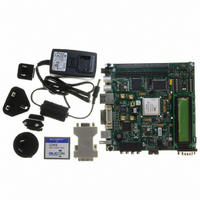
ML501 Platform, DVI Adapter and CompactFlash Card
Silicon Manufacturer
Xilinx
Features
Programmable System Clock Generator Chip, RS-232 Serial Port
Silicon Family Name
Virtex-5
Silicon Core Number
XC5VLX50FFG676
Lead Free Status / RoHS Status
Lead free / RoHS Compliant
For Use With/related Products
XC5VLX50FFG676
Lead Free Status / RoHS Status
Lead free / RoHS Compliant, Lead free / RoHS Compliant
Other names
122-1508
Available stocks
Company
Part Number
Manufacturer
Quantity
Price


Chapter 1: ML501 Evaluation Platform
16
2. DDR2 SODIMM
3. Differential Clock Input And Output With SMA Connectors
MIG Compliance
DDR2 Memory Expansion
DDR2 Clock Signal
DDR2 Signaling
The ML501 platform is shipped with a single-rank unregistered 256 MB SODIMM. The
DDR2 SODIMM used is generally a Micron MT4HTF3264HY-53E or similar module. Serial
Presence Detect (SPD) using an IIC interface to the DDR DIMM is also supported with the
FPGA.
Note:
rates might be possible but are not tested.
The ML50x DDR2 interface is MIG pinout compliant. The MIG DDR2 routing guidelines
outlined in the Xilinx Memory Interface Generator (MIG) User Guide
achieved.
The board’s DDR2 SODIMM memory interface is designed to the requirements defined by
the MIG User Guide using the MIG tool. The MIG documentation requires that designers
follow the MIG pinout and layout guidelines. The MIG tool generates and ensures that the
proper FPGA I/O pin selections are made in support of the board’s DDR2 interface. The
initial pin selection for the board was modified and then re-verified to meet the MIG
pinout requirements. To ensure a robust interface, the ML50x DDR2 layout incorporates
matched trace lengths for data signals to the corresponding data strobe signal as defined in
the MIG user guide. See
about MIG and Virtex-5 FPGAs in general.
The DDR2 interface support user installation of SODIMM modules with more memory
since higher order address and chip select signals are also routed from the SODIMM to the
FPGA.
Two matched length pairs of DDR2 clock signals are broadcast from the FPGA to the
SODIMM. The FPGA design is responsible for driving both clock pairs with low skew. The
delay on the clock trace is designed to match the delay of the other DDR2 control signals.
All DDR2 SDRAM control signals are terminated through 47Ω resistors to a 0.9V VTT
reference voltage. The FPGA DDR2 interface supports SSTL18 signaling and all DDR2
signals are controlled impedance. The DDR2 data, mask, and strobe signals are matched
length within byte groups. The ODT functionality of the SODIMM should be utilized.
High-precision clock signals can be input to the FPGA using differential clock signals
brought in through 50Ω SMA connectors. This allows an external function generator or
other clock source to drive the differential clock inputs that directly feed the global clock
input pins of the FPGA. The FPGA can be configured to present a 100Ω termination
impedance.
The board is only tested for DDR2 SDRAM operation at a 400 MHz data rate. Faster data
Appendix B, “References”
www.xilinx.com
for links to additional information
UG226 (v1.4) August 24, 2009
ML501 Evaluation Platform
[Ref 13]
have been
R
Related parts for HW-V5-ML501-UNI-G
Image
Part Number
Description
Manufacturer
Datasheet
Request
R

Part Number:
Description:
IC CPLD .8K 36MCELL 44-VQFP
Manufacturer:
Xilinx Inc
Datasheet:

Part Number:
Description:
IC CPLD 72MCRCELL 10NS 44VQFP
Manufacturer:
Xilinx Inc
Datasheet:

Part Number:
Description:
IC CPLD 1.6K 72MCELL 64-VQFP
Manufacturer:
Xilinx Inc
Datasheet:

Part Number:
Description:
IC CR-II CPLD 64MCELL 44-VQFP
Manufacturer:
Xilinx Inc
Datasheet:

Part Number:
Description:
IC CPLD 1.6K 72MCELL 100-TQFP
Manufacturer:
Xilinx Inc
Datasheet:

Part Number:
Description:
IC CR-II CPLD 64MCELL 56-BGA
Manufacturer:
Xilinx Inc
Datasheet:

Part Number:
Description:
IC CPLD 72MCRCELL 7.5NS 44VQFP
Manufacturer:
Xilinx Inc
Datasheet:
Part Number:
Description:
IC CR-II CPLD 64MCELL 100-VQFP
Manufacturer:
Xilinx Inc
Datasheet:
Part Number:
Description:
IC CPLD 1.6K 72MCELL 100-TQFP
Manufacturer:
Xilinx Inc
Datasheet:

Part Number:
Description:
IC CPLD 72MCRCELL 7.5NS 64VQFP
Manufacturer:
Xilinx Inc
Datasheet:
Part Number:
Description:
IC CPLD 1.6K 72MCELL 100-TQFP
Manufacturer:
Xilinx Inc
Datasheet:

Part Number:
Description:
IC CPLD 1.5K 64MCELL HP 44-VQFP
Manufacturer:
Xilinx Inc

Part Number:
Description:
IC CPLD 36MCRCELL 15NS 44PLCC
Manufacturer:
Xilinx Inc
Datasheet:

Part Number:
Description:
IC CPLD 36MCRCELL 10NS 44PLCC
Manufacturer:
Xilinx Inc
Datasheet:

Part Number:
Description:
IC CPLD 1.5K 64MCELL HP 44-VQFP
Manufacturer:
Xilinx Inc