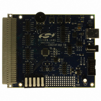
C8051F360-TB Silicon Laboratories Inc, C8051F360-TB Datasheet - Page 243

C8051F360-TB
Manufacturer Part Number
C8051F360-TB
Description
BOARD TARGET/PROTO W/C8051F360
Manufacturer
Silicon Laboratories Inc
Type
MCUr
Specifications of C8051F360-TB
Contents
Board
Processor To Be Evaluated
C8051F36x
Interface Type
USB
Lead Free Status / RoHS Status
Lead free / RoHS Compliant
For Use With/related Products
C8051F360
Lead Free Status / Rohs Status
Lead free / RoHS Compliant
Other names
336-1412
- Current page: 243 of 288
- Download datasheet (3Mb)
Bits 7–0: SCR7–SCR0: SPI0 Clock Rate.
Example: If SYSCLK = 2 MHz and SPI0CKR = 0x04,
SFR Page:
SFR Address:
f
Bits 7–0: SPI0DAT: SPI0 Transmit and Receive Data.
SFR Page:
SFR Address:
SCK
SCR7
f
SCK
R/W
Bit7
R/W
Bit7
=
=
These bits determine the frequency of the SCK output when the SPI0 module is configured
for master mode operation. The SCK clock frequency is a divided version of the system
clock, and is given in the following equation, where SYSCLK is the system clock frequency
and SPI0CKR is the 8-bit value held in the SPI0CKR register.
for 0 <= SPI0CKR <= 255
f
200kHz
SCK
all pages
0xA2
The SPI0DAT register is used to transmit and receive SPI0 data. Writing data to SPI0DAT
places the data into the transmit buffer and initiates a transfer when in Master Mode. A read
of SPI0DAT returns the contents of the receive buffer.
------------------------- -
2
all pages
0xA3
2000000
SCR6
×
R/W
Bit6
(
=
R/W
Bit6
4
+
------------------------------------------------ -
2
×
1
SFR Definition 20.3. SPI0CKR: SPI0 Clock Rate
)
(
SPI0CKR
SCR5
SYSCLK
R/W
Bit5
SFR Definition 20.4. SPI0DAT: SPI0 Data
R/W
Bit5
SCR4
+
R/W
Bit4
1
R/W
Bit4
)
C8051F360/1/2/3/4/5/6/7/8/9
SCR3
Rev. 1.0
R/W
Bit3
R/W
Bit3
SCR2
R/W
Bit2
R/W
Bit2
SCR1
R/W
Bit1
R/W
Bit1
SCR0
R/W
Bit0
R/W
Bit0
00000000
Reset Value
00000000
Reset Value
243
Related parts for C8051F360-TB
Image
Part Number
Description
Manufacturer
Datasheet
Request
R
Part Number:
Description:
SMD/C°/SINGLE-ENDED OUTPUT SILICON OSCILLATOR
Manufacturer:
Silicon Laboratories Inc
Part Number:
Description:
Manufacturer:
Silicon Laboratories Inc
Datasheet:
Part Number:
Description:
N/A N/A/SI4010 AES KEYFOB DEMO WITH LCD RX
Manufacturer:
Silicon Laboratories Inc
Datasheet:
Part Number:
Description:
N/A N/A/SI4010 SIMPLIFIED KEY FOB DEMO WITH LED RX
Manufacturer:
Silicon Laboratories Inc
Datasheet:
Part Number:
Description:
N/A/-40 TO 85 OC/EZLINK MODULE; F930/4432 HIGH BAND (REV E/B1)
Manufacturer:
Silicon Laboratories Inc
Part Number:
Description:
EZLink Module; F930/4432 Low Band (rev e/B1)
Manufacturer:
Silicon Laboratories Inc
Part Number:
Description:
I°/4460 10 DBM RADIO TEST CARD 434 MHZ
Manufacturer:
Silicon Laboratories Inc
Part Number:
Description:
I°/4461 14 DBM RADIO TEST CARD 868 MHZ
Manufacturer:
Silicon Laboratories Inc
Part Number:
Description:
I°/4463 20 DBM RFSWITCH RADIO TEST CARD 460 MHZ
Manufacturer:
Silicon Laboratories Inc
Part Number:
Description:
I°/4463 20 DBM RADIO TEST CARD 868 MHZ
Manufacturer:
Silicon Laboratories Inc
Part Number:
Description:
I°/4463 27 DBM RADIO TEST CARD 868 MHZ
Manufacturer:
Silicon Laboratories Inc
Part Number:
Description:
I°/4463 SKYWORKS 30 DBM RADIO TEST CARD 915 MHZ
Manufacturer:
Silicon Laboratories Inc
Part Number:
Description:
N/A N/A/-40 TO 85 OC/4463 RFMD 30 DBM RADIO TEST CARD 915 MHZ
Manufacturer:
Silicon Laboratories Inc
Part Number:
Description:
I°/4463 20 DBM RADIO TEST CARD 169 MHZ
Manufacturer:
Silicon Laboratories Inc


