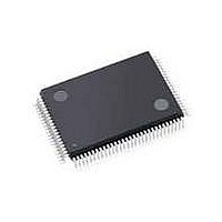
C8051F040-TB Silicon Laboratories Inc, C8051F040-TB Datasheet - Page 222

C8051F040-TB
Manufacturer Part Number
C8051F040-TB
Description
BOARD PROTOTYPING W/C8051F040
Manufacturer
Silicon Laboratories Inc
Type
MCUr
Specifications of C8051F040-TB
Contents
Board
Processor To Be Evaluated
C8051F04x
Interface Type
USB
Lead Free Status / RoHS Status
Contains lead / RoHS non-compliant
For Use With/related Products
C8051F040
Lead Free Status / Rohs Status
Lead free / RoHS Compliant
- Current page: 222 of 328
- Download datasheet (3Mb)
C8051F040/1/2/3/4/5/6/7
222
Bits7-0:
Bits7-0:
P4.7
R/W
R/W
Bit7
Bit7
P4.[7:0]: Port4 Output Latch Bits.
Write - Output appears on I/O pins.
0: Logic Low Output.
1: Logic High Output (Open-Drain if corresponding P4MDOUT.n bit = 0). See SFR Definition
17.17.
Read - Returns states of I/O pins.
0: P4.n pin is logic low.
1: P4.n pin is logic high.
Note: P4.7 (/WR), P4.6 (/RD), and P4.5 (ALE) can be driven by the External Data Memory
Interface. See
page 187
P4MDOUT.[7:0]: Port4 Output Mode Bits.
0: Port Pin output mode is configured as Open-Drain.
1: Port Pin output mode is configured as Push-Pull.
P4.6
R/W
R/W
Bit6
Bit6
SFR Definition 17.17. P4MDOUT: Port4 Output Mode
for more information.
Section “16. External Data Memory Interface and On-Chip XRAM” on
P4.5
R/W
R/W
Bit5
Bit5
SFR Definition 17.16. P4: Port4 Data
P4.4
R/W
R/W
Bit4
Bit4
Rev. 1.5
P4.3
R/W
R/W
Bit3
Bit3
P4.2
R/W
R/W
Bit2
Bit2
P4.1
R/W
R/W
Bit1
Bit1
SFR Address:
SFR Address:
SFR Page:
SFR Page:
P4.0
R/W
R/W
Bit0
Bit0
0xC8
F
0x9C
F
Addressable
Reset Value
00000000
Reset Value
11111111
Bit
Related parts for C8051F040-TB
Image
Part Number
Description
Manufacturer
Datasheet
Request
R
Part Number:
Description:
SMD/C°/SINGLE-ENDED OUTPUT SILICON OSCILLATOR
Manufacturer:
Silicon Laboratories Inc
Part Number:
Description:
Manufacturer:
Silicon Laboratories Inc
Datasheet:
Part Number:
Description:
N/A N/A/SI4010 AES KEYFOB DEMO WITH LCD RX
Manufacturer:
Silicon Laboratories Inc
Datasheet:
Part Number:
Description:
N/A N/A/SI4010 SIMPLIFIED KEY FOB DEMO WITH LED RX
Manufacturer:
Silicon Laboratories Inc
Datasheet:
Part Number:
Description:
N/A/-40 TO 85 OC/EZLINK MODULE; F930/4432 HIGH BAND (REV E/B1)
Manufacturer:
Silicon Laboratories Inc
Part Number:
Description:
EZLink Module; F930/4432 Low Band (rev e/B1)
Manufacturer:
Silicon Laboratories Inc
Part Number:
Description:
I°/4460 10 DBM RADIO TEST CARD 434 MHZ
Manufacturer:
Silicon Laboratories Inc
Part Number:
Description:
I°/4461 14 DBM RADIO TEST CARD 868 MHZ
Manufacturer:
Silicon Laboratories Inc
Part Number:
Description:
I°/4463 20 DBM RFSWITCH RADIO TEST CARD 460 MHZ
Manufacturer:
Silicon Laboratories Inc
Part Number:
Description:
I°/4463 20 DBM RADIO TEST CARD 868 MHZ
Manufacturer:
Silicon Laboratories Inc
Part Number:
Description:
I°/4463 27 DBM RADIO TEST CARD 868 MHZ
Manufacturer:
Silicon Laboratories Inc
Part Number:
Description:
I°/4463 SKYWORKS 30 DBM RADIO TEST CARD 915 MHZ
Manufacturer:
Silicon Laboratories Inc
Part Number:
Description:
N/A N/A/-40 TO 85 OC/4463 RFMD 30 DBM RADIO TEST CARD 915 MHZ
Manufacturer:
Silicon Laboratories Inc
Part Number:
Description:
I°/4463 20 DBM RADIO TEST CARD 169 MHZ
Manufacturer:
Silicon Laboratories Inc


