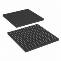
MPC8308-RDB Freescale Semiconductor, MPC8308-RDB Datasheet - Page 62

MPC8308-RDB
Manufacturer Part Number
MPC8308-RDB
Description
BOARD REF DESIGN MPC8308
Manufacturer
Freescale Semiconductor
Series
PowerQUICC II™ PROr
Type
MPUr
Datasheets
1.MPC8308VMAGD.pdf
(90 pages)
2.MPC8308VMAGD.pdf
(2 pages)
3.MPC8308-RDB.pdf
(36 pages)
4.MPC8308-RDB.pdf
(2 pages)
Specifications of MPC8308-RDB
Contents
Board, Cables, Documentation, Power Supply, Software
Ethernet Connection Type
Serial to Ethernet
Data Rate
10 Mbps, 100 Mbps, 1000 Mbps
Memory Type
DDR2, SDRAM
Interface Type
HSSI
Operating Voltage
1.5 V
Operating Current
5 uA
Maximum Power Dissipation
1000 mW
Operating Temperature Range
- 55 C to + 125 C
Product
Modules
For Use With/related Products
MPC8308
Lead Free Status / RoHS Status
Lead free / RoHS Compliant
SPI
19.2
Table 52
Figure 49
Figure 50
generally reference the rising edge of the clock, these AC timing diagrams also apply when the falling edge
is the active edge.
62
SPI outputs valid—master mode (internal clock) delay
SPI outputs hold—master mode (internal clock) delay
SPI outputs valid—slave mode (external clock) delay
SPI outputs hold—slave mode (external clock) delay
SPI inputs—master mode (internal clock) input setup time
SPI inputs—master mode (internal clock) input hold time
SPI inputs—slave mode (external clock) input setup time
SPI inputs—slave mode (external clock) input hold time
Notes:
1. Output specifications are measured from the 50% level of the rising edge of SPICLK to the 50% level of the signal. Timings
2. The symbols used for timing specifications follow the pattern of t
are measured at the pin.
inputs and t
timing (NI) for the time SPICLK clock reference (K) goes to the high state (H) until outputs (O) are invalid (X).
and provide the SPI input and output AC timing specifications.
SPI AC Timing Specifications
provides the AC test load for the SPI.
Output high voltage
Output low voltage
Output low voltage
through
(first two letters of functional block)(reference)(state)(signal)(state)
Characteristic
Figure 51
MPC8308 PowerQUICC II Pro Processor Hardware Specification, Rev. 2
Output
Characteristic
Table 51. SPI DC Electrical Characteristics (continued)
represent the AC timing from
Table 52. SPI AC Timing Specifications
Symbol
V
V
V
Figure 49. SPI AC Test Load
OH
OL
OL
Z
0
= 50 Ω
I
I
OH
I
OL
OL
Condition
= –8.0 mA
= 3.2 mA
= 8.0 mA
(first two letters of functional block)(signal)(state)(reference)(state)
for outputs. For example, t
Table
R
52. Note that although the specifications
L
Symbol
t
t
t
t
t
t
NEKHOV
NEKHOX
t
t
= 50 Ω
Min
NIKHOV
NIKHOX
NEIVKH
NEIXKH
2.4
NIIVKH
NIIXKH
—
—
1
2
NV
Max
0.5
0.4
NIKHOX
DD
—
Min
0.5
—
2
6
0
4
2
/2
Freescale Semiconductor
symbolizes the internal
Unit
Max
8.5
V
V
V
—
—
—
—
—
—
6
Unit
ns
ns
ns
ns
ns
ns
ns
ns
for


