5.07.01 FLASHER ARM Segger Microcontroller Systems, 5.07.01 FLASHER ARM Datasheet - Page 44
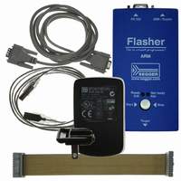
5.07.01 FLASHER ARM
Manufacturer Part Number
5.07.01 FLASHER ARM
Description
PROGRAMMER JTAG FOR ARM CORES
Manufacturer
Segger Microcontroller Systems
Type
In-System Programmerr
Specifications of 5.07.01 FLASHER ARM
Contents
Programmer
For Use With/related Products
ARM7, ARM9, Cortex
Lead Free Status / RoHS Status
Lead free / RoHS Compliant
Other names
899-1002


44
5.2
5.2.1
Flasher ARM (UM08007)
The J-Link and J-Trace JTAG is also compatible to
ARM’s Serial Wire Debug (SWD).
The following table lists the J-Link / J-Trace SWD
pinout.
Table 5.3: J-Link / J-Trace SWD pinout
Pins 4, 6, 8, 10, 12, 14, 16, 18, 20 are GND pins connected to GND in J-Link. They
should also be connected to GND in the target system.
11
13
15
17
19
PIN
1
2
3
5
7
9
Using the JTAG connector with SWD
Pin Out
VTref
Vsupply
Not Used NC
Not used NC
SWDIO
SWCLK
Not used NC
SWO
RESET
Not used NC
5V-Tar-
get sup-
ply
SIGNAL
Input
NC
I/O
Output
Output
I/O
Output
TYPE
This is the target reference voltage. It is used to check if
the target has power, to create the logic-level reference for
the input comparators and to control the output logic levels
to the target. It is normally fed from Vdd of the target board
and must not have a series resistor.
This pin is not connected in J-Link. It is reserved for com-
patibility with other equipment. Connect to Vdd or leave
open in target system.
This pin is not used by J-Link. If the device may also be
accessed via JTAG, this pin may be connected to nTRST,
otherwise leave open.
This pin is not used by J-Link. If the device may also be
accessed via JTAG, this pin may be connected to TDI, oth-
erwise leave open.
Single bi-directional data pin.
Clock signal to target CPU.
It is recommended that this pin is pulled to a defined state
of the target board. Typically connected to TCK of target
CPU.
This pin is not used by J-Link. This pin is not used by J-Link
when operating in SWD mode. If the device may also be
accessed via JTAG, this pin may be connected to RTCK, oth-
erwise leave open.
Serial Wire Output trace port. (Optional, not required for
SWD communication.)
Target CPU reset signal. Typically connected to the RESET
pin of the target CPU, which is typically called "nRST",
"nRESET" or "RESET".
This pin is not connected in J-Link.
This pin is used to supply power to some eval boards. Not
all J-Links supply power on this pin, only the KS (Kickstart)
versions. Typically left open on target hardware.
CHAPTER 5
© 2004-2009 SEGGER Microcontroller GmbH & Co. KG
Description
SWO
RESET
Not used
V5-Supply
VTref
Not used
Not used
SWDIO
SWCLK
Not used
11
13
15
17
19
1
3
5
7
9
2
12
4
6
8
10
14
16
18
20
Vsupply
GND
GND
GND
GND
GND
GND
GND
GND
GND
Hardware
Related parts for 5.07.01 FLASHER ARM
Image
Part Number
Description
Manufacturer
Datasheet
Request
R

Part Number:
Description:
CONNECTOR JTAG-ARM ISOLATION
Manufacturer:
Segger Microcontroller Systems
Datasheet:

Part Number:
Description:
ADAPTER ARM TARGET 14PIN RIBBON
Manufacturer:
Segger Microcontroller Systems
Datasheet:

Part Number:
Description:
JTAG EMULATOR FOR ARM CORES
Manufacturer:
Segger Microcontroller Systems
Datasheet:

Part Number:
Description:
JTAG EMULATOR FOR ARM CORES
Manufacturer:
Segger Microcontroller Systems
Datasheet:

Part Number:
Description:
PROGRAMMING TOOL FOR MCU
Manufacturer:
Segger Microcontroller Systems
Datasheet:

Part Number:
Description:
PROGRAMMING TOOL FOR ST7 MCU
Manufacturer:
Segger Microcontroller Systems
Datasheet:

Part Number:
Description:
PROGRAMMING TOOL FOR STM8
Manufacturer:
Segger Microcontroller Systems
Datasheet:

Part Number:
Description:
JTAG EMULATOR USB ETHERNET ARM
Manufacturer:
Segger Microcontroller Systems
Datasheet:

Part Number:
Description:
JTAG EMULATOR ARM7/ARM9 ETM
Manufacturer:
Segger Microcontroller Systems
Datasheet:

Part Number:
Description:
EMULATOR JTAG/SWD CORTEX M3
Manufacturer:
Segger Microcontroller Systems
Datasheet: