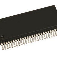
KIT33927EKEVBE Freescale Semiconductor, KIT33927EKEVBE Datasheet - Page 25

KIT33927EKEVBE
Manufacturer Part Number
KIT33927EKEVBE
Description
KIT EVALUATION FOR MC33927
Manufacturer
Freescale Semiconductor
Series
SMARTMOS™r
Type
Other Power Managementr
Datasheet
1.KIT33927EKEVBE.pdf
(44 pages)
Specifications of KIT33927EKEVBE
Main Purpose
Power Management, FET Driver (External FET)
Embedded
No
Utilized Ic / Part
MC33927
Primary Attributes
*
Secondary Attributes
8 V ~ 40 V Supply
Interface Type
SPI
Product
Power Management Modules
Silicon Manufacturer
Freescale
Silicon Core Number
MC33927
Kit Application Type
Power Management
Application Sub Type
FET Driver
Kit Contents
Board, CD
Rohs Compliant
Yes
Lead Free Status / RoHS Status
Lead free / RoHS Compliant
For Use With/related Products
MC33927
on this pin, typically 15V. Higher voltages on the pin
increases the IC power dissipation.
This limits the gate voltage capable of being applied to the
FETs and reduces system performance due to the higher
FET on-resistance. To allow a higher gate voltage to be
supplied, the IC also incorporates a charge pump. The
switches and control circuitry are internal; the capacitors and
diodes are external (see
LOW SIDE DRIVERS
FETs. The circuits provide a low impedance drive to the gate,
ensuring the FETs remain off in the presence of high dV/dt
transients on their drains. Additionally, these output drivers
isolate the other portions of the IC from currents capable of
being injected into the substrate due to rapid dV/dt transients
on the FET drains.
low-side FETs. The low-side drivers are capable of providing
a typical peak current of 2.0A. This gate drive current may be
limited by external resistors in order to achieve a good trade-
off between the efficiency and EMC (Electro-Magnetic
Compatibility) compliance of the application. the low side
driver uses high side PMOS for turn on and low side isolated
LDMOS for turn off. The circuit ensures the impedance of the
driver remains low, even during periods of reduced current.
Current limit is blanked immediately after subsequent input
state change in order to ensure device stays off during dV/dt
transients.
HIGH SIDE DRIVERS
bootstrap capacitor to the external high side FETs. The
circuits provide a low-impedance drive to the gate, ensuring
the FETs remain off in the presence of high dV/dt transients
on their sources. Further, these output drivers isolate the
other portions of the IC from currents capable of being
injected into the substrate due to rapid dV/dt transients on the
FETs.
capacitor to the gate of the external high-side FET, thus
turning the high-side FET on. The high-side driver uses a
level shifter, which allows the gate of the external high-side
FET to be turned off by switching to the high-side FET
source.
is obtained from the bootstrap supply, a short time is required
after the application of power to the IC to charge the
bootstrap capacitors. To ensure this occurrence, the internal
control logic will not allow a high-side switch to be turned on
after entering the ENABLE state until the corresponding low
side switch is enabled at least once. Caution must be
exercised after a long period of inactivity of the low-side
switches, to verify the bootstrap capacitor is not discharged.
Analog Integrated Circuit Device Data
Freescale Semiconductor
In 12V systems the supply voltage can fall as low as 6.0V.
These three drivers turn on and off the external low side
Low-side drivers switch power from VLS to the gates of the
These three drivers switch the voltage across the
The high-side drivers deliver power from their bootstrap
Because the gate supply voltage for the high-side drivers
Figure
17).
It can be recharged by activating the low-side switches for a
brief period, or by attaching external bleed resistors to the
HS_S pins to GND.
high-side external FETs, a fully integrated trickle charge
pump provides the charge necessary to fully enhance the
external FET gates.
driver output impedance, overall (external and internal) gate
resistance and the load capacitance. To ensure the low-side
FET is not turned on by a large positive dV/dt on the drain of
the low side FET, the turn-on slew rate of the high-side
should be limited. If the slew rate of the high side is limited by
the gate-drain capacitance of the high side FET, then the
displacement current injected into the low-side gate drive
output will be approximately the same value. Therefore, to
ensure the low side drivers can be held off, the voltage drop
across the low side gate driver must be lower than the
threshold voltage of the low side FET (see
will be able to remain off if its gate drive low side switch,
develops a voltage drop less than the threshold voltage of the
high side FET. The gate drive low side switch discharges the
gate to the source.
could be forced below ground. The low side FETs must not
inject detrimental substrate currents in this condition.
the load current during switching.
In order to achieve a 100% duty cycle operation of the
The slew rate of the external output FET is limited by the
Similarly, during large negative dV/dt, the high side FET
Additionally, during negative dV/dt the low side gate drive
The occurrence of these cases depends on the polarity of
Figure 12. Positive DV/dt Transient
FUNCTIONAL INTERNAL BLOCK DESCRIPTION
Figure
INTRODUCTION
12).
33927
25


