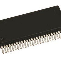
KIT33927EKEVBE Freescale Semiconductor, KIT33927EKEVBE Datasheet - Page 8

KIT33927EKEVBE
Manufacturer Part Number
KIT33927EKEVBE
Description
KIT EVALUATION FOR MC33927
Manufacturer
Freescale Semiconductor
Series
SMARTMOS™r
Type
Other Power Managementr
Datasheet
1.KIT33927EKEVBE.pdf
(44 pages)
Specifications of KIT33927EKEVBE
Main Purpose
Power Management, FET Driver (External FET)
Embedded
No
Utilized Ic / Part
MC33927
Primary Attributes
*
Secondary Attributes
8 V ~ 40 V Supply
Interface Type
SPI
Product
Power Management Modules
Silicon Manufacturer
Freescale
Silicon Core Number
MC33927
Kit Application Type
Power Management
Application Sub Type
FET Driver
Kit Contents
Board, CD
Rohs Compliant
Yes
Lead Free Status / RoHS Status
Lead free / RoHS Compliant
For Use With/related Products
MC33927
Table 3. Static Electrical Characteristics
values noted reflect the approximate parameter means at T
8
33927
ELECTRICAL CHARACTERISTICS
STATIC ELECTRICAL CHARACTERISTICS
POWER INPUTS
VDD V INTERNAL REGULATOR
VLS REGULATOR
Notes
VBAT Supply Voltage Startup Threshold
VBAT Supply Current, V
VPWR Supply Current, V
Sleep State Supply Current, RST = 0V
Sleep State Output Gate Voltage
Trickle Charge Pump (Bootstrap Voltage)
Bootstrap Diode Forward Voltage at 10mA
V
Internal V
Peak Output Current, V
Linear Regulator Output Voltage, I
VLS Disable Threshold
10.
11.
12.
Characteristics noted under conditions 8.0V ≤ V
DD
8.
9.
RST and ENABLE = 5.0V
No output loads on Gate Drive Pins, No PWM
No output loads on Gate Drive Pins, 20kHz, 50% Duty Cycle
RST and ENABLE = 5.0V
No output loads on Gate Drive Pins, No PWM
Output Loads = 620nC per FET, 20kHz PWM
V
V
IG < 100µA
V
External Load I
BAT
PWR
BAT
Output Voltage, V
When minimum system voltage could be less than 14V operation with the Charge Pump is recommended. V
threshold in order for the Charge Pump and V
will continue to operate even if V
This parameter is guaranteed by design. It is not production tested.
Minimum external capacitor for stable V
Recommended external capacitor for the V
When V
= 40V
= 14V
= 40V
DD
Supply Current, V
LS
is less than this value, the outputs are disabled and HOLDOFF circuits are active.
DD_EXT
PWR
(12)
PWR
PWR
PWR
= 0 to 1.0mA
= 8V to 40V, C = 0.47µF
Characteristic
= 16V, V
= V
= V
DD
BAT
BAT
= 5.5V, No External Load
VLS
= 40V
LS
= 40V
= 0 to 60mA
BAT
= 10V
(8)
STATIC ELECTRICAL CHARACTERISTICS
drops below 6.0V.
DD
(9)
operation is 0.47µF.
LS
(11)
(10)
DD
regulator is 2.2µF low ESR at each pin VLS and VLS_CAP.
PWR
regulator to startup and drive V
= V
BAT
A
= 25°C under nominal conditions unless otherwise noted.
≤ 40V, -40°C ≤ T
V
I
Symbol
V
V
PWR_ON
GATESS
BAT_ST
V
I
I
PEAK
THVLS
I
I
V
PWR
V
I
BAT
BAT
V
Boot
DD
DD
LS
F
PWR
A
≤ 125°C, unless otherwise noted. Typical
to > 8.0V. Once V
13.5
Min
350
4.5
7.5
22
–
–
–
–
–
–
–
–
–
–
Analog Integrated Circuit Device Data
Typ
600
6.0
1.0
8.0
11
14
56
28
15
–
–
–
–
–
–
PWR
Freescale Semiconductor
exceeds 8.0V, the circuits
BAT
must exceed this
Max
100
800
8.0
1.3
1.2
5.5
8.5
10
20
95
30
32
12
17
–
Unit
mA
mA
mA
mA
µA
V
V
V
V
V
V
V


