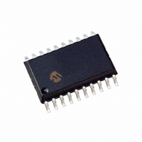
PIC16F690-I/SO Microchip Technology, PIC16F690-I/SO Datasheet - Page 103

PIC16F690-I/SO
Manufacturer Part Number
PIC16F690-I/SO
Description
IC PIC MCU FLASH 4KX14 20SOIC
Manufacturer
Microchip Technology
Series
PIC® 16Fr
Datasheets
1.PIC16F616T-ISL.pdf
(8 pages)
2.PIC16F690DM-PCTLHS.pdf
(306 pages)
3.PIC16F677-IP.pdf
(2 pages)
4.PIC16F677-IP.pdf
(16 pages)
5.PIC16F677-ISO.pdf
(294 pages)
Specifications of PIC16F690-I/SO
Program Memory Type
FLASH
Program Memory Size
7KB (4K x 14)
Package / Case
20-SOIC (7.5mm Width)
Core Processor
PIC
Core Size
8-Bit
Speed
20MHz
Connectivity
I²C, SPI, UART/USART
Peripherals
Brown-out Detect/Reset, POR, PWM, WDT
Number Of I /o
18
Eeprom Size
256 x 8
Ram Size
256 x 8
Voltage - Supply (vcc/vdd)
2 V ~ 5.5 V
Data Converters
A/D 12x10b
Oscillator Type
Internal
Operating Temperature
-40°C ~ 85°C
Processor Series
PIC16F
Core
PIC
Data Bus Width
8 bit
Data Ram Size
256 B
Interface Type
I2C/SPI/SSP/EUSART
Maximum Clock Frequency
20 MHz
Number Of Programmable I/os
17
Number Of Timers
3
Operating Supply Voltage
2 V to 5.5 V
Maximum Operating Temperature
+ 85 C
Mounting Style
SMD/SMT
3rd Party Development Tools
52715-96, 52716-328, 52717-734
Development Tools By Supplier
PG164130, DV164035, DV244005, DV164005, PG164120, ICE2000, DM163014, DM164120-1, DM163029
Minimum Operating Temperature
- 40 C
On-chip Adc
12-ch x 10-bit
Data Rom Size
256 B
A/d Bit Size
10 bit
A/d Channels Available
12
Height
2.31 mm
Length
12.8 mm
Supply Voltage (max)
5.5 V
Supply Voltage (min)
4.5 V
Width
7.49 mm
Lead Free Status / RoHS Status
Lead free / RoHS Compliant
For Use With
XLT20SO1-1 - SOCKET TRANS ICE 20DIP TO 20SOICPIC16F690DM-PCTLHS - BOARD DEMO PICTAIL HUMIDITY SNSRAC162061 - HEADER INTRFC MPLAB ICD2 20PINAC164039 - MODULE SKT PROMATE II 20DIP/SOIC
Lead Free Status / Rohs Status
Lead free / RoHS Compliant
Available stocks
Company
Part Number
Manufacturer
Quantity
Price
Company:
Part Number:
PIC16F690-I/SO
Manufacturer:
Multicomp
Quantity:
60 000
Part Number:
PIC16F690-I/SO
Manufacturer:
MICREL/麦瑞
Quantity:
20 000
8.8
There are three additional comparator features:
• Timer1 count enable (gate)
• Synchronizing output with Timer1
• Simultaneous read of comparator outputs
8.8.1
This feature can be used to time the duration or interval
of analog events. Clearing the T1GSS bit of the
CM2CON1 register will enable Timer1 to increment
based on the output of Comparator C2. This requires
that Timer1 is on and gating is enabled. See
Section 6.0 “Timer1 Module with Gate Control” for
details.
It is recommended to synchronize the comparator with
Timer1 by setting the C2SYNC bit when the comparator
is used as the Timer1 gate source. This ensures Timer1
does not miss an increment if the comparator changes
during an increment.
REGISTER 8-3:
© 2006 Microchip Technology Inc.
bit 7
Legend:
R = Readable bit
-n = Value at POR
bit 7
bit 6
bit 5-2
bit 1
bit 0
Note 1:
MC1OUT
R-0
2:
Additional Comparator Features
Refer to Section 6.6 “Timer1 Gate”.
Refer to Figure 8-3.
COMPARATOR C2 GATING TIMER1
MC1OUT: Mirror Copy of C1OUT bit
MC2OUT: Mirror Copy of C2OUT bit
Unimplemented: Read as ‘0’
T1GSS: Timer1 Gate Source Select bit
1 = Timer1 gate source is T1G
0 = Timer1 gate source is SYNCC2OUT.
C2SYNC: Comparator C2 Output Synchronization bit
1 = Output is synchronous to falling edge of Timer1 clock
0 = Output is asynchronous
MC2OUT
R-0
CM2CON1: COMPARATOR C2 CONTROL REGISTER 1
W = Writable bit
‘1’ = Bit is set
U-0
PIC16F631/677/685/687/689/690
—
U-0
Preliminary
—
(1)
U = Unimplemented bit, read as ‘0’
‘0’ = Bit is cleared
8.8.2
The Comparator C2 output can be synchronized with
Timer1 by setting the C2SYNC bit of the CM2CON1
register. When enabled, the C2 output is latched on the
falling edge of the Timer1 clock source. If a prescaler is
used with Timer1, the comparator output is latched after
the prescaling function. To prevent a race condition, the
comparator output is latched on the falling edge of the
Timer1 clock source and Timer1 increments on the
rising edge of its clock source. See the Comparator
Block Diagram (Figure 8-3) and the Timer1 Block
Diagram (Figure 6-1) for more information.
8.8.3
The MC1OUT and MC2OUT bits of the CM2CON1
register are mirror copies of both comparator outputs.
The ability to read both outputs simultaneously from a
single register eliminates the timing skew of reading
separate registers.
U-0
—
Note 1: Obtaining the status of C1OUT or C2OUT
(2)
SYNCHRONIZING COMPARATOR
C2 OUTPUT TO TIMER1
SIMULTANEOUS COMPARATOR
OUTPUT READ
by reading CM2CON1 does not affect the
comparator interrupt mismatch registers.
U-0
—
x = Bit is unknown
T1GSS
R/W-1
DS41262C-page 101
C2SYNC
R/W-0
bit 0


