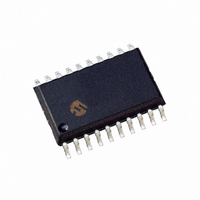
PIC16F690-I/SO Microchip Technology, PIC16F690-I/SO Datasheet - Page 61

PIC16F690-I/SO
Manufacturer Part Number
PIC16F690-I/SO
Description
IC PIC MCU FLASH 4KX14 20SOIC
Manufacturer
Microchip Technology
Series
PIC® 16Fr
Datasheets
1.PIC16F616T-ISL.pdf
(8 pages)
2.PIC16F690DM-PCTLHS.pdf
(306 pages)
3.PIC16F677-IP.pdf
(2 pages)
4.PIC16F677-IP.pdf
(16 pages)
5.PIC16F677-ISO.pdf
(294 pages)
Specifications of PIC16F690-I/SO
Program Memory Type
FLASH
Program Memory Size
7KB (4K x 14)
Package / Case
20-SOIC (7.5mm Width)
Core Processor
PIC
Core Size
8-Bit
Speed
20MHz
Connectivity
I²C, SPI, UART/USART
Peripherals
Brown-out Detect/Reset, POR, PWM, WDT
Number Of I /o
18
Eeprom Size
256 x 8
Ram Size
256 x 8
Voltage - Supply (vcc/vdd)
2 V ~ 5.5 V
Data Converters
A/D 12x10b
Oscillator Type
Internal
Operating Temperature
-40°C ~ 85°C
Processor Series
PIC16F
Core
PIC
Data Bus Width
8 bit
Data Ram Size
256 B
Interface Type
I2C/SPI/SSP/EUSART
Maximum Clock Frequency
20 MHz
Number Of Programmable I/os
17
Number Of Timers
3
Operating Supply Voltage
2 V to 5.5 V
Maximum Operating Temperature
+ 85 C
Mounting Style
SMD/SMT
3rd Party Development Tools
52715-96, 52716-328, 52717-734
Development Tools By Supplier
PG164130, DV164035, DV244005, DV164005, PG164120, ICE2000, DM163014, DM164120-1, DM163029
Minimum Operating Temperature
- 40 C
On-chip Adc
12-ch x 10-bit
Data Rom Size
256 B
A/d Bit Size
10 bit
A/d Channels Available
12
Height
2.31 mm
Length
12.8 mm
Supply Voltage (max)
5.5 V
Supply Voltage (min)
4.5 V
Width
7.49 mm
Lead Free Status / RoHS Status
Lead free / RoHS Compliant
For Use With
XLT20SO1-1 - SOCKET TRANS ICE 20DIP TO 20SOICPIC16F690DM-PCTLHS - BOARD DEMO PICTAIL HUMIDITY SNSRAC162061 - HEADER INTRFC MPLAB ICD2 20PINAC164039 - MODULE SKT PROMATE II 20DIP/SOIC
Lead Free Status / Rohs Status
Lead free / RoHS Compliant
Available stocks
Company
Part Number
Manufacturer
Quantity
Price
Company:
Part Number:
PIC16F690-I/SO
Manufacturer:
Multicomp
Quantity:
60 000
Part Number:
PIC16F690-I/SO
Manufacturer:
MICREL/麦瑞
Quantity:
20 000
4.0
There are as many as eighteen general purpose I/O
pins available. Depending on which peripherals are
enabled, some or all of the pins may not be available as
general purpose I/O. In general, when a peripheral is
enabled, the associated pin may not be used as a
general purpose I/O pin.
4.1
PORTA is a 6-bit wide, bidirectional port. The
corresponding data direction register is TRISA
(Register 4-2). Setting a TRISA bit (= 1) will make the
corresponding PORTA pin an input (i.e., disable the
output driver). Clearing a TRISA bit (= 0) will make the
corresponding PORTA pin an output (i.e., enables
output driver and puts the contents of the output latch
on the selected pin). The exception is RA3, which is
input only and its TRIS bit will always read as ‘1’.
Example 4-1 shows how to initialize PORTA.
Reading the PORTA register (Register 4-1) reads the
status of the pins, whereas writing to it will write to the
PORT latch. All write operations are read-modify-write
operations. Therefore, a write to a port implies that the
REGISTER 4-1:
REGISTER 4-2:
© 2006 Microchip Technology Inc.
bit 7
Legend:
R = Readable bit
-n = Value at POR
bit 7-6
bit 5-0
bit 7
Legend:
R = Readable bit
-n = Value at POR
bit 7-6
bit 5-0
Note 1:
U-0
U-0
—
—
2:
I/O PORTS
PORTA and the TRISA Registers
TRISA<3> always reads ‘1’.
TRISA<5:4> always reads ‘1’ in XT, HS and LP Oscillator modes.
Unimplemented: Read as ‘0’
RA<5:0>: PORTA I/O Pin bit
1 = Port pin is > V
0 = Port pin is < V
Unimplemented: Read as ‘0’
TRISA<5:0>: PORTA Tri-State Control bit
1 = PORTA pin configured as an input (tri-stated)
0 = PORTA pin configured as an output
U-0
U-0
—
—
PORTA: PORTA REGISTER
TRISA: PORTA TRI-STATE REGISTER
W = Writable bit
‘1’ = Bit is set
W = Writable bit
‘1’ = Bit is set
IH
IL
TRISA5
R/W-1
R/W-x
RA5
PIC16F631/677/685/687/689/690
TRISA4
R/W-x
R/W-1
RA4
Preliminary
U = Unimplemented bit, read as ‘0’
‘0’ = Bit is cleared
U = Unimplemented bit, read as ‘0’
‘0’ = Bit is cleared
TRISA3
port pins are read, this value is modified and then
written to the PORT data latch. RA3 reads ‘0’ when
MCLRE = 1.
The TRISA register controls the PORTA pin output
drivers, even when they are being used as analog
inputs. The user should ensure the bits in the TRISA
register are maintained set when using them as analog
inputs. I/O pins configured as analog input always read
‘0’.
EXAMPLE 4-1:
RA3
R-x
R-1
BCF
BCF
CLRF
BSF
CLRF
BSF
BCF
MOVLW 0Ch
MOVWF TRISA
BCF
Note:
STATUS,RP0
STATUS,RP1
PORTA
STATUS,RP1
ANSEL
STATUS,RP0
STATUS,RP1
STATUS,RP0
The ANSEL register must be initialized to
configure an analog channel as a digital
input. Pins configured as analog inputs will
read ‘0’.
TRISA2
R/W-1
R/W-x
RA2
;Bank 0
;
;Init PORTA
;Bank 2
;digital I/O
;Bank 1
;
;Set RA<3:2> as inputs
;and set RA<5:4,1:0>
;as outputs
;Bank 0
INITIALIZING PORTA
x = Bit is unknown
x = Bit is unknown
TRISA1
R/W-1
R/W-x
RA1
DS41262C-page 59
TRISA0
R/W-x
R/W-1
RA0
bit 0
bit 0


