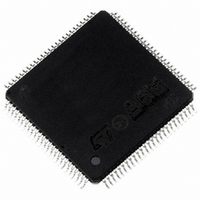
ST92F150CV1TB STMicroelectronics, ST92F150CV1TB Datasheet - Page 141

ST92F150CV1TB
Manufacturer Part Number
ST92F150CV1TB
Description
MCU 8BIT 128K FLASH 100TQFP
Manufacturer
STMicroelectronics
Series
ST9r
Datasheet
1.ST92F150CV1TB.pdf
(429 pages)
Specifications of ST92F150CV1TB
Core Processor
ST9
Core Size
8/16-Bit
Speed
24MHz
Connectivity
CAN, EBI/EMI, I²C, LIN, SCI, SPI
Peripherals
DMA, LVD, POR, PWM, WDT
Number Of I /o
77
Program Memory Size
128KB (128K x 8)
Program Memory Type
FLASH
Eeprom Size
1K x 8
Ram Size
4K x 8
Voltage - Supply (vcc/vdd)
4.5 V ~ 5.5 V
Data Converters
A/D 16x10b
Oscillator Type
Internal
Operating Temperature
-40°C ~ 105°C
Package / Case
100-TQFP, 100-VQFP
Processor Series
ST92F15x
Core
ST9
Data Bus Width
8 bit, 16 bit
Data Ram Size
6 KB
Interface Type
CAN, I2C, SCI, SPI
Maximum Clock Frequency
24 MHz
Number Of Programmable I/os
80
Number Of Timers
5 x 16 bit
Operating Supply Voltage
4.5 V to 5.5 V
Maximum Operating Temperature
+ 105 C
Mounting Style
SMD/SMT
Development Tools By Supplier
ST92F150-EPB
Minimum Operating Temperature
- 40 C
On-chip Adc
16 bit x 10 bit
Lead Free Status / RoHS Status
Lead free / RoHS Compliant
Other names
497-4883
Available stocks
Company
Part Number
Manufacturer
Quantity
Price
Company:
Part Number:
ST92F150CV1TB
Manufacturer:
STMicroelectronics
Quantity:
10 000
- Current page: 141 of 429
- Download datasheet (8Mb)
RESET/STOP MANAGER (Cont’d)
The on-chip Timer/Watchdog generates a reset
condition if the Watchdog mode is enabled
(WCR.WDGEN cleared, R252 page 0), and if the
programmed period elapses without the specific
code (AAh, 55h) written to the appropriate register.
The input pin RESET is not driven low by the on-
chip reset generated by the Timer/Watchdog.
When the Reset pin goes high again, 20479 oscil-
lator clock cycles (CLOCK1) are counted before ex-
iting the Reset state (+ one possible CLOCK1 pe-
riod, depending on the delay between the rising
edge of the Reset pin and the first rising edge of
CLOCK1). Subsequently a short Boot routine is ex-
ecuted from the device internal Boot memory, and
control then passes to the user program.
The Boot routine sets the device characteristics
and loads the correct values in the Memory Man-
agement Unit’s pointer registers, so that these
point to the physical memory areas as mapped in
the specific device. The precise duration of this
short Boot routine varies from device to device,
depending on the Boot memory contents.
At the end of the Boot routine the Program Coun-
ter will be set to the location specified in the Reset
Vector located in the lowest two bytes of memory.
7.6.1 Reset Pin Timing
To improve the noise immunity of the device, the
Reset pin has a Schmitt trigger input circuit with
hysteresis. In addition, a filter will prevent an un-
wanted reset in case of a single glitch of less than
50 ns on the Reset pin. The device is certain to re-
set if a negative pulse of more than 20μs is ap-
plied. When the reset pin goes high again, a delay
Figure 72. Reset Pin Input Structure
PIN
ST92F124/F150/F250 - RESET AND CLOCK CONTROL UNIT (RCCU)
ESD PROTECTION
CIRCUITRY
TO GENERATE RESET SIGNAL
SCHMITT TRIGGER and LOW
of up to 4μs will elapse before the RCCU detects
this rising front. From this event on, a defined
number of CLOCK1 cycles (refer to t
counted before exiting the Reset state (+ one pos-
sible CLOCK1 period depending on the delay be-
tween the positive edge the RCCU detects and the
first rising edge of CLOCK1).
If the ST9 is a ROMLESS version, without on-chip
program memory, the memory interface ports are
set to external memory mode (i.e Alternate Func-
tion) and the memory accesses are made to exter-
nal Program memory with wait cycles insertion.
If the Voltage Regulator is present in the device,
please ensure the reset pin is released only when
the internal voltage supply is stabilized at 3.3V.
Figure 71. Recommended Signal to be Applied
on Reset Pin
V
V
V
RESETN
IHRS
ILRS
V
DD
PASS FILTER
Minimum
20μs
RSPH
141/429
) is
9
Related parts for ST92F150CV1TB
Image
Part Number
Description
Manufacturer
Datasheet
Request
R

Part Number:
Description:
BOARD PROGRAM FOR ST92F150 MCU
Manufacturer:
STMicroelectronics
Datasheet:

Part Number:
Description:
BOARD EVALUATION FOR ST9 SERIES
Manufacturer:
STMicroelectronics
Datasheet:

Part Number:
Description:
BOARD EMULATOR FOR ST9 SERIES
Manufacturer:
STMicroelectronics
Datasheet:

Part Number:
Description:
MCU, MPU & DSP Development Tools ST9 Dedication Board
Manufacturer:
STMicroelectronics
Datasheet:

Part Number:
Description:
STMicroelectronics [RIPPLE-CARRY BINARY COUNTER/DIVIDERS]
Manufacturer:
STMicroelectronics
Datasheet:

Part Number:
Description:
STMicroelectronics [LIQUID-CRYSTAL DISPLAY DRIVERS]
Manufacturer:
STMicroelectronics
Datasheet:

Part Number:
Description:
BOARD EVAL FOR MEMS SENSORS
Manufacturer:
STMicroelectronics
Datasheet:

Part Number:
Description:
NPN TRANSISTOR POWER MODULE
Manufacturer:
STMicroelectronics
Datasheet:

Part Number:
Description:
TURBOSWITCH ULTRA-FAST HIGH VOLTAGE DIODE
Manufacturer:
STMicroelectronics
Datasheet:

Part Number:
Description:
Manufacturer:
STMicroelectronics
Datasheet:

Part Number:
Description:
DIODE / SCR MODULE
Manufacturer:
STMicroelectronics
Datasheet:

Part Number:
Description:
DIODE / SCR MODULE
Manufacturer:
STMicroelectronics
Datasheet:


