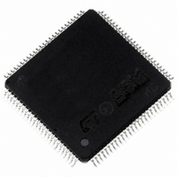
ST92F150CV1TB STMicroelectronics, ST92F150CV1TB Datasheet - Page 272

ST92F150CV1TB
Manufacturer Part Number
ST92F150CV1TB
Description
MCU 8BIT 128K FLASH 100TQFP
Manufacturer
STMicroelectronics
Series
ST9r
Datasheet
1.ST92F150CV1TB.pdf
(429 pages)
Specifications of ST92F150CV1TB
Core Processor
ST9
Core Size
8/16-Bit
Speed
24MHz
Connectivity
CAN, EBI/EMI, I²C, LIN, SCI, SPI
Peripherals
DMA, LVD, POR, PWM, WDT
Number Of I /o
77
Program Memory Size
128KB (128K x 8)
Program Memory Type
FLASH
Eeprom Size
1K x 8
Ram Size
4K x 8
Voltage - Supply (vcc/vdd)
4.5 V ~ 5.5 V
Data Converters
A/D 16x10b
Oscillator Type
Internal
Operating Temperature
-40°C ~ 105°C
Package / Case
100-TQFP, 100-VQFP
Processor Series
ST92F15x
Core
ST9
Data Bus Width
8 bit, 16 bit
Data Ram Size
6 KB
Interface Type
CAN, I2C, SCI, SPI
Maximum Clock Frequency
24 MHz
Number Of Programmable I/os
80
Number Of Timers
5 x 16 bit
Operating Supply Voltage
4.5 V to 5.5 V
Maximum Operating Temperature
+ 105 C
Mounting Style
SMD/SMT
Development Tools By Supplier
ST92F150-EPB
Minimum Operating Temperature
- 40 C
On-chip Adc
16 bit x 10 bit
Lead Free Status / RoHS Status
Lead free / RoHS Compliant
Other names
497-4883
Available stocks
Company
Part Number
Manufacturer
Quantity
Price
Company:
Part Number:
ST92F150CV1TB
Manufacturer:
STMicroelectronics
Quantity:
10 000
- Current page: 272 of 429
- Download datasheet (8Mb)
I2C BUS INTERFACE
I
10.8.6.1 DMA between Peripheral and Register
File
If the DMA transaction is made between the pe-
ripheral and the Register File, one register is
required to hold the DMA Address and one to hold
the DMA transaction counter.
These two registers must be located in the Regis-
ter File:
– the DMA Address Register in the even ad-
– the DMA Transaction Counter in the following
They are pointed to by the DMA Transaction
Counter Pointer Register (I2CRDC register in re-
ceiving, I2CTDC register in transmitting) located in
the peripheral register page.
In order to select the DMA transaction with the
Register File, the control bit I2CRDC.RF/MEM in
receiving mode or I2CTDC.RF/MEM in transmit-
ting mode must be set.
The transaction Counter Register must be initial-
ized with the number of DMA transfers to perform
and will be decremented after each transaction.
The DMA Address Register must be initialized with
the starting address of the DMA table in the Regis-
ter File, and it is increased after each transaction.
These two registers must be located between ad-
dresses 00h and DFh of the Register File.
When the DMA occurs between Peripheral and
Register File, the I2CTDAP register (in transmis-
sion) and the I2CRDAP one (in reception) are not
used.
10.8.6.2 DMA between Peripheral and Memory
Space
If the DMA transaction is made between the pe-
ripheral and Memory, a register pair is required to
hold the DMA Address and another register pair to
hold the DMA Transaction counter. These two
pairs of registers must be located in the Register
File. The DMA Address pair is pointed to by the
DMA Address Pointer Register (I2CRDAP register
in reception, I2CTDAP register in transmission) lo-
cated in the peripheral register page; the DMA
Transaction Counter pair is pointed to by the DMA
Transaction Counter Pointer Register (I2CRDC
register in reception, I2CTDC register in transmis-
sion) located in the peripheral register page.
In order to select the DMA transaction with the
Memory Space, the control bit I2CRDC.RF/MEM
in receiving mode or I2CTDC.RF/MEM in transmit-
ting mode must be reset.
272/429
9
2
C BUS INTERFACE (Cont’d)
dressed register,
register (odd address).
The Transaction Counter registers pair must be in-
itialized with the number of DMA transfers to per-
form and will be decremented after each transac-
tion. The DMA Address register pair must be ini-
tialized with the starting address of the DMA table
in the Memory Space, and it is increased after
each transaction. These two register pairs must be
located between addresses 00h and DFh of the
Register File.
10.8.6.3 DMA in Master Receive
To correctly manage the reception of the last byte
when the DMA in Master Receive mode is used,
the following sequence of operations must be per-
formed:
1. The number of data bytes to be received must
2. When the Receiving End Of Block condition
The last byte of the reception sequence can be re-
ceived either using interrupts/polling or using
DMA. If the user wants to receive the last byte us-
ing DMA, the number of bytes to be received must
be set to 1, and the DMA in reception must be re-
enabled (IMR.RXDM bit set) to receive the last
byte. Moreover the Receiving End Of Block inter-
rupt service routine must be designed to recognize
and manage the two different End Of Block situa-
tions (after the first sequence of data bytes and af-
ter the last data byte).
be set to the effective number of bytes minus
one byte.
occurs, the I2CCR.STOP bit must be set and
the I2CCR.ACK bit must be reset.
Related parts for ST92F150CV1TB
Image
Part Number
Description
Manufacturer
Datasheet
Request
R

Part Number:
Description:
BOARD PROGRAM FOR ST92F150 MCU
Manufacturer:
STMicroelectronics
Datasheet:

Part Number:
Description:
BOARD EVALUATION FOR ST9 SERIES
Manufacturer:
STMicroelectronics
Datasheet:

Part Number:
Description:
BOARD EMULATOR FOR ST9 SERIES
Manufacturer:
STMicroelectronics
Datasheet:

Part Number:
Description:
MCU, MPU & DSP Development Tools ST9 Dedication Board
Manufacturer:
STMicroelectronics
Datasheet:

Part Number:
Description:
STMicroelectronics [RIPPLE-CARRY BINARY COUNTER/DIVIDERS]
Manufacturer:
STMicroelectronics
Datasheet:

Part Number:
Description:
STMicroelectronics [LIQUID-CRYSTAL DISPLAY DRIVERS]
Manufacturer:
STMicroelectronics
Datasheet:

Part Number:
Description:
BOARD EVAL FOR MEMS SENSORS
Manufacturer:
STMicroelectronics
Datasheet:

Part Number:
Description:
NPN TRANSISTOR POWER MODULE
Manufacturer:
STMicroelectronics
Datasheet:

Part Number:
Description:
TURBOSWITCH ULTRA-FAST HIGH VOLTAGE DIODE
Manufacturer:
STMicroelectronics
Datasheet:

Part Number:
Description:
Manufacturer:
STMicroelectronics
Datasheet:

Part Number:
Description:
DIODE / SCR MODULE
Manufacturer:
STMicroelectronics
Datasheet:

Part Number:
Description:
DIODE / SCR MODULE
Manufacturer:
STMicroelectronics
Datasheet:


