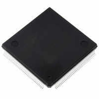
ST10R167-Q3 STMicroelectronics, ST10R167-Q3 Datasheet - Page 13

ST10R167-Q3
Manufacturer Part Number
ST10R167-Q3
Description
IC MCU 16BIT ROMLESS 144-PQFP
Manufacturer
STMicroelectronics
Series
ST10r
Datasheet
1.ST10R167-Q3.pdf
(63 pages)
Specifications of ST10R167-Q3
Core Processor
ST10
Core Size
16-Bit
Speed
25MHz
Connectivity
CAN, EBI/EMI, SSC, UART/USART
Peripherals
POR, PWM, WDT
Number Of I /o
111
Program Memory Type
ROMless
Ram Size
4K x 8
Voltage - Supply (vcc/vdd)
4.5 V ~ 5.5 V
Data Converters
A/D 16x10b
Oscillator Type
Internal
Operating Temperature
-40°C ~ 125°C
Package / Case
144-QFP
Processor Series
ST10R1x
Core
ST10
Data Bus Width
16 bit
Program Memory Size
32 KB
Data Ram Size
4 KB
Interface Type
CAN/SSC/USART
Maximum Clock Frequency
25 MHz
Number Of Programmable I/os
111
Number Of Timers
5
Maximum Operating Temperature
+ 125 C
Mounting Style
SMD/SMT
Minimum Operating Temperature
- 40 C
On-chip Adc
16-ch x 10-bit
Lead Free Status / RoHS Status
Lead free / RoHS Compliant
Eeprom Size
-
Program Memory Size
-
Lead Free Status / Rohs Status
Lead free / RoHS Compliant
Other names
497-2043
Available stocks
Company
Part Number
Manufacturer
Quantity
Price
Company:
Part Number:
ST10R167-Q3
Manufacturer:
ST
Quantity:
556
Company:
Part Number:
ST10R167-Q3
Manufacturer:
STMicroelectronics
Quantity:
10 000
Part Number:
ST10R167-Q3
Manufacturer:
ST
Quantity:
20 000
Company:
Part Number:
ST10R167-Q3/TR
Manufacturer:
STMicroelectronics
Quantity:
10 000
Company:
Part Number:
ST10R167-Q3B0
Manufacturer:
ST
Quantity:
1 343
Part Number:
ST10R167-Q3B0
Manufacturer:
ST
Quantity:
20 000
VI - EXTERNAL BUS CONTROLLER
All of the external memory accesses are per-
formed by the on-chip external bus controller. The
EBC can be programmed to single chip mode
when no external memory is required, or to one of
four different external memory access modes:
– 16-/18-/20-/24-bit addresses and 16-bit data,
– 16-/18-/20-/24-bit addresses and 16-bit data,
– 16-/18-/20-/24-bit addresses and 8-bit data,
– 16-/18-/20-/24-bit addresses and 8-bit data, de-
In demultiplexed bus modes addresses are output
on Port1 and data is input/output on Port0 or P0L,
respectively. In the multiplexed bus modes both
addresses and data use Port0 for input/output.
Timing characteristics of the external bus inter-
face (memory cycle time, memory tri-state time,
length of ALE and read/write delay) are program-
mable giving the choice of a wide range of memo-
ries and external peripherals. Up to 4 independent
address windows may be defined (using register
pairs ADDRSELx / BUSCONx) to access different
resources and bus characteristics. These address
windows
BUSCON4 overrides BUSCON3 and BUSCON2
overrides BUSCON1. All accesses to locations
not covered by these 4 address windows are con-
trolled by BUSCON0. Up to 5 external CS signals
(4 windows plus default) can be generated in
order to save external glue logic. Access to very
slow memories is supported by a ‘Ready’ function.
demultiplexed.
multiplexed.
multiplexed.
multiplexed.
are
arranged
hierarchically
where
A HOLD/HLDA protocol is available for bus arbi-
tration which shares external resources with other
bus masters. The bus arbitration is enabled by
setting bit HLDEN in register SYSCON. After set-
ting HLDEN once, pins P6.7...P6.5 (BREQ,
HLDA, HOLD) are automatically controlled by the
EBC. In master mode (default after reset) the
HLDA pin is an output. By setting bit DP6.7 to’1’
the slave mode is selected where pin HLDA is
switched to input. This directly connects the slave
controller to another master controller without
glue logic.
For applications which require less external mem-
ory space, the address space can be restricted to
1M Byte, 256K Byte or to 64K Byte. Port 4 outputs
all 8 address lines if an address space of
16M Byte is used, otherwise four, two or no
address lines.
Chip select timing can be made programmable.
By default (after reset), the CSx lines change half
a CPU clock cycle after the rising edge of ALE.
With the CSCFG bit set in the SYSCON register
the CSx lines change with the rising edge of ALE.
The active level of the READY pin can be set by
bit RDYPOL in the BUSCONx registers. When the
READY function is enabled for a specific address
window, each bus cycle within the window must
be terminated with the active level defined by bit
RDYPOL in the associated BUSCON register.
ST10R167
13/63


