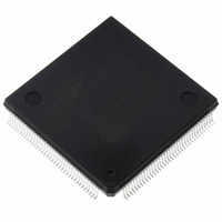
ST10R167-Q3 STMicroelectronics, ST10R167-Q3 Datasheet - Page 23

ST10R167-Q3
Manufacturer Part Number
ST10R167-Q3
Description
IC MCU 16BIT ROMLESS 144-PQFP
Manufacturer
STMicroelectronics
Series
ST10r
Datasheet
1.ST10R167-Q3.pdf
(63 pages)
Specifications of ST10R167-Q3
Core Processor
ST10
Core Size
16-Bit
Speed
25MHz
Connectivity
CAN, EBI/EMI, SSC, UART/USART
Peripherals
POR, PWM, WDT
Number Of I /o
111
Program Memory Type
ROMless
Ram Size
4K x 8
Voltage - Supply (vcc/vdd)
4.5 V ~ 5.5 V
Data Converters
A/D 16x10b
Oscillator Type
Internal
Operating Temperature
-40°C ~ 125°C
Package / Case
144-QFP
Processor Series
ST10R1x
Core
ST10
Data Bus Width
16 bit
Program Memory Size
32 KB
Data Ram Size
4 KB
Interface Type
CAN/SSC/USART
Maximum Clock Frequency
25 MHz
Number Of Programmable I/os
111
Number Of Timers
5
Maximum Operating Temperature
+ 125 C
Mounting Style
SMD/SMT
Minimum Operating Temperature
- 40 C
On-chip Adc
16-ch x 10-bit
Lead Free Status / RoHS Status
Lead free / RoHS Compliant
Eeprom Size
-
Program Memory Size
-
Lead Free Status / Rohs Status
Lead free / RoHS Compliant
Other names
497-2043
Available stocks
Company
Part Number
Manufacturer
Quantity
Price
Company:
Part Number:
ST10R167-Q3
Manufacturer:
ST
Quantity:
556
Company:
Part Number:
ST10R167-Q3
Manufacturer:
STMicroelectronics
Quantity:
10 000
Part Number:
ST10R167-Q3
Manufacturer:
ST
Quantity:
20 000
Company:
Part Number:
ST10R167-Q3/TR
Manufacturer:
STMicroelectronics
Quantity:
10 000
Company:
Part Number:
ST10R167-Q3B0
Manufacturer:
ST
Quantity:
1 343
Part Number:
ST10R167-Q3B0
Manufacturer:
ST
Quantity:
20 000
XII - A/D CONVERTER
A10-bit A/D converter with 16 multiplexed input
channels and a sample and hold circuit is inte-
grated on-chip. The sample time (for loading the
capacitors) and the conversion time is program-
mable and can be adjusted to the external circuitry.
Overrun error detection/protection is controlled by
the ADDAT register. Either an interrupt request is
generated when the result of a previous conver-
sion has not been read from the result register at
the time the next conversion is complete, or the
next conversion is suspended until the previous
result has been read. For applications which
require less than 16 analog input channels, the
remaining channel inputs can be used as digital
input port pins. The AD converter
ST10F168 supports different conversion modes :
– Single channel single conversion : the analog
– Single channel continuous conversion : the
– Auto scan single conversion : the analog level
– Auto scan continuous conversion : the ana-
– Wait for ADDAT read mode : when using con-
Table 9 : ADC sample clock and conversion time
Note
level of the selected channel is sampled once
and converted. The result of the conversion is
stored in the ADDAT register.
analog level of the selected channel is repeatedly
sampled and converted. The result of the conver-
sion is stored in the ADDAT register.
of the selected channels are sampled once and
converted. After each conversion the result is
stored in the ADDAT register. The data can be
transfered to the RAM by interrupt software
management or using the powerfull Peripheral
Event Controller data transfert.
log level of the selected channels are repeatedly
sampled and converted. The result of the con-
version is stored in the ADDAT register. The
data can be transfered to the RAM by interrupt
software management or using the powerfull
Peripheral Event Controller data transfert.
tinuous modes, in order to avoid to overwrite
the result of the current conversion by the next
one, the ADWR bit of ADCON control register
ADCTC
00
01
10
11
1. See chapter XX.
2. t
CC
= TCL x 24.
Reserved, do not use
TCL
1
TCL x 24
TCL x 96
TCL x 48
= 1/2 x f
Conversion Clock t
XTAL
At f
CPU
CC
0.48 s
1.92 s
0.96 s
of the
= 25MHz
-
– Channel
The Table : 9 ADC sample clock and conversion
time shows the ADC unit conversion clock, sample
clock.
A complete conversion will take 14t
4 TCL. This time includes the conversion it-self,
the sampling time and the time required to trans-
fer the digital value to the result register. For
example, at 25MHz of CPU clock, minimum com-
plete conversion time is 7.76 s.
The A/D converter provides automatic offset and
linearity self calibration. The calibration operation
is performed in two ways:
– A full calibration sequence is performed after a
– One calibration cycle is performed after each
must be activated. Then, until the ADDAT regis-
ter is read, the new result is stored in a tempo-
rary buffer and the conversion is on hold.
continuous modes, a selected channel can be
converted in between without changing the
current operating mode. The 10 bit data of the
conversion are stored in ADRES field of
ADDAT2. The current continuous mode remains
active after the single conversion is completed.
reset and lasts 1.6ms minimum (at 25MHz CPU
clock). During this time, the ADBSY flag is set to
indicate the operation. Normal conversion can
be performed during this time. The duration of
the calibration sequence is then extended by the
time consumed by the conversions.
Note : After a power-on reset, the total
unadjusted error (TUE) of the ADC might be
worse than ±2LSB (max. ±4LSB). During the full
calibration sequence, the TUE is constantly
improved until at the end of the cycle, TUE is
within the specified limits of ±2LSB.
conversion : each calibration cycle takes 4 ADC
clock cycles. These operation cycles ensure
constant updating of the ADC accuracy, com-
pensating changing operating conditions.
ADSTC
00
01
10
11
injection
t
t
t
CC
CC
CC
t
CC
-
x 2
x 4
x 8
Sample Clock t
mode
:
At f
when
CC
CPU
ST10R167
0.48 s
0.96 s
1.92 s
3.84 s
SC
+ 2 t
= 25MHz
2
2
2
2
using
23/63
SC
+


