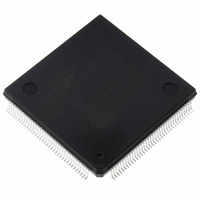
ST10R167-Q3 STMicroelectronics, ST10R167-Q3 Datasheet - Page 42

ST10R167-Q3
Manufacturer Part Number
ST10R167-Q3
Description
IC MCU 16BIT ROMLESS 144-PQFP
Manufacturer
STMicroelectronics
Series
ST10r
Datasheet
1.ST10R167-Q3.pdf
(63 pages)
Specifications of ST10R167-Q3
Core Processor
ST10
Core Size
16-Bit
Speed
25MHz
Connectivity
CAN, EBI/EMI, SSC, UART/USART
Peripherals
POR, PWM, WDT
Number Of I /o
111
Program Memory Type
ROMless
Ram Size
4K x 8
Voltage - Supply (vcc/vdd)
4.5 V ~ 5.5 V
Data Converters
A/D 16x10b
Oscillator Type
Internal
Operating Temperature
-40°C ~ 125°C
Package / Case
144-QFP
Processor Series
ST10R1x
Core
ST10
Data Bus Width
16 bit
Program Memory Size
32 KB
Data Ram Size
4 KB
Interface Type
CAN/SSC/USART
Maximum Clock Frequency
25 MHz
Number Of Programmable I/os
111
Number Of Timers
5
Maximum Operating Temperature
+ 125 C
Mounting Style
SMD/SMT
Minimum Operating Temperature
- 40 C
On-chip Adc
16-ch x 10-bit
Lead Free Status / RoHS Status
Lead free / RoHS Compliant
Eeprom Size
-
Program Memory Size
-
Lead Free Status / Rohs Status
Lead free / RoHS Compliant
Other names
497-2043
Available stocks
Company
Part Number
Manufacturer
Quantity
Price
Company:
Part Number:
ST10R167-Q3
Manufacturer:
ST
Quantity:
556
Company:
Part Number:
ST10R167-Q3
Manufacturer:
STMicroelectronics
Quantity:
10 000
Part Number:
ST10R167-Q3
Manufacturer:
ST
Quantity:
20 000
Company:
Part Number:
ST10R167-Q3/TR
Manufacturer:
STMicroelectronics
Quantity:
10 000
Company:
Part Number:
ST10R167-Q3B0
Manufacturer:
ST
Quantity:
1 343
Part Number:
ST10R167-Q3B0
Manufacturer:
ST
Quantity:
20 000
ST10R167
XX - ELECTRICAL CHARACTERISTICS (continued)
XX.4.1 - Definition of internal timing
The internal operation of the ST10C167 is
controlled by the internal CPU clock f
edges of the CPU clock can trigger internal (e.g.
pipeline) or external (e.g. bus cycles) operations.
The specification of the external timing (AC
Characteristics) therefore depends on the time
between two consecutive edges of the CPU clock,
called “TCL” periods (see Figure 11).
The CPU clock signal can be generated by
different mechanisms. The duration of TCL
periods and their variation (and also the derived
external timing) depends on the mechanism used
Figure 11 : Generation mechanisms for the CPU clock
Table 17 : CPU Frequency Generation
Notes 1. The external clock input range refers to a CPU clock range of 10...25MHz.
42/63
1
1
1
1
0
0
0
0
(P0H.7-5)
P0.15-13
2. The maximum frequency depends on the duty cycle of the external clock signal.
1
1
0
0
1
1
0
0
1
0
1
0
1
0
1
0
Phase locked loop operation
Direct Clock Drive
Prescaler Operation
CPU Frequency f
f
f
f
f
f
f
XTAL
CPU
XTAL
CPU
XTAL
CPU
F
F
F
F
F
F
F
F
XTAL
XTAL
XTAL
XTAL
XTAL
XTAL
XTAL
XTAL
x 1.5
x 2.5
CPU
x 4
x 3
x 2
x 5
x 1
/ 2
= f
CPU
XTAL
. Both
x F
External Clock Input Range
to generate f
when calculating the timings for the ST10C167.
The example for PLL operation shown in
Figure 11 refers to a PLL factor of 4.
The mechanism used to generate the CPU clock
is selected during reset by the logic levels on pins
P0.15-13 (P0H.7-5).
XX.4.2 - Clock generation modes
Table 18
combinations of these three bits with the
respective clock generation mode.
3.33 to 8.33MHz
6.66 to 16.6MHz
2.5 to 6.25MHz
5 to 12.5MHz
1 to 25MHz
2 to 50MHz
4 to 10MHz
2 to 5MHz
shows
CPU
TCL
. This influence must be regarded
TCL
the
TCL TCL
TCL TCL
1
association
Default configuration
Direct drive
CPU clock via prescaler
Notes
2
of
the


