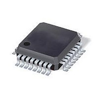
ST7FLI49MK1T6 STMicroelectronics, ST7FLI49MK1T6 Datasheet - Page 15

ST7FLI49MK1T6
Manufacturer Part Number
ST7FLI49MK1T6
Description
MCU 8BIT SGL VOLT FLASH 32-LQFP
Manufacturer
STMicroelectronics
Series
ST7r
Datasheet
1.ST7FLI49MK1T6TR.pdf
(187 pages)
Specifications of ST7FLI49MK1T6
Core Processor
ST7
Core Size
8-Bit
Speed
8MHz
Connectivity
I²C
Peripherals
LVD, POR, PWM, WDT
Number Of I /o
24
Program Memory Size
4KB (4K x 8)
Program Memory Type
FLASH
Eeprom Size
128 x 8
Ram Size
384 x 8
Voltage - Supply (vcc/vdd)
2.4 V ~ 5.5 V
Data Converters
A/D 10x10b
Oscillator Type
Internal
Operating Temperature
-40°C ~ 85°C
Package / Case
32-LQFP
Processor Series
ST7FLI4x
Core
ST7
Data Bus Width
8 bit
Data Ram Size
384 B
Interface Type
I2C
Maximum Clock Frequency
8 MHz
Number Of Programmable I/os
24
Number Of Timers
5
Maximum Operating Temperature
+ 125 C
Mounting Style
SMD/SMT
Minimum Operating Temperature
- 40 C
On-chip Adc
10 bit, 10 Channel
Lead Free Status / RoHS Status
Lead free / RoHS Compliant
Available stocks
Company
Part Number
Manufacturer
Quantity
Price
Company:
Part Number:
ST7FLI49MK1T6
Manufacturer:
st
Quantity:
456
Company:
Part Number:
ST7FLI49MK1T6
Manufacturer:
STMicroelectronics
Quantity:
10 000
Part Number:
ST7FLI49MK1T6
Manufacturer:
ST
Quantity:
20 000
Company:
Part Number:
ST7FLI49MK1T6TR
Manufacturer:
STMicroelectronics
Quantity:
10 000
ST7LITE49M
Table 2.
10
11
12
13
number
1
2
3
4
5
6
8
9
Pin
10
12
13
14
15
16
17
5
6
7
8
9
PA3(HS)/ATPWM1
PA5 (HS)ATPWM3
Legend / Abbreviations for
Type: I = input, O = output, S = supply
In/Output level: C
Output level: HS = 20 mA high sink (on N-buffer only)
Port and control configuration:
●
●
The RESET configuration of each pin is shown in bold which is valid as long as the device is
in reset state.
Device pin description
PA7(HS)/I2CCLK
ATPWM2/MCO
OSC1/CLKIN
Pin name
PA4(HS)/
PA6(HS)/
I2CDATA
Input: float = floating, wpu = weak pull-up, int = interrupt, ana = analog
Output: OD = open-drain, PP = push-pull
RESET
V
V
V
V
OSC2
SSA
DDA
DD
SS
(2)
(2)
(2)
(2)
T
= CMOS 0.3V
I/O
I/O
I/O
I/O
I/O
O
S
S
S
S
I
C
C
C
C
C
Level
T
T
T
T
T
Table
HS
HS
HS
HS
HS
Doc ID 13562 Rev 3
2:
DD
/0.7V
x
x
x
x
x
DD
x
Input
ei0
with input trigger
Port/control
ei0
Output
T
T
x
x
x
x
x
x
x
Resonator oscillator output
inverter input or external
function
Port A3
Port A4
Port A5
Port A6
Port A7
Analog ground voltage
Analog supply voltage
Digital ground voltage
Digital supply voltage
reset)
(after
Main
Resonator oscillator
(HS)
(HS)
(HS)
(HS)
(HS)
clock input
Pin description
Reset
ATPWM2/
Alternate
ATPWM1
ATPWM3
function
I2CDATA
I2CCLK
MCO
15/188


