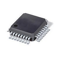
ST7FLI49MK1T6 STMicroelectronics, ST7FLI49MK1T6 Datasheet - Page 25

ST7FLI49MK1T6
Manufacturer Part Number
ST7FLI49MK1T6
Description
MCU 8BIT SGL VOLT FLASH 32-LQFP
Manufacturer
STMicroelectronics
Series
ST7r
Datasheet
1.ST7FLI49MK1T6TR.pdf
(187 pages)
Specifications of ST7FLI49MK1T6
Core Processor
ST7
Core Size
8-Bit
Speed
8MHz
Connectivity
I²C
Peripherals
LVD, POR, PWM, WDT
Number Of I /o
24
Program Memory Size
4KB (4K x 8)
Program Memory Type
FLASH
Eeprom Size
128 x 8
Ram Size
384 x 8
Voltage - Supply (vcc/vdd)
2.4 V ~ 5.5 V
Data Converters
A/D 10x10b
Oscillator Type
Internal
Operating Temperature
-40°C ~ 85°C
Package / Case
32-LQFP
Processor Series
ST7FLI4x
Core
ST7
Data Bus Width
8 bit
Data Ram Size
384 B
Interface Type
I2C
Maximum Clock Frequency
8 MHz
Number Of Programmable I/os
24
Number Of Timers
5
Maximum Operating Temperature
+ 125 C
Mounting Style
SMD/SMT
Minimum Operating Temperature
- 40 C
On-chip Adc
10 bit, 10 Channel
Lead Free Status / RoHS Status
Lead free / RoHS Compliant
Available stocks
Company
Part Number
Manufacturer
Quantity
Price
Company:
Part Number:
ST7FLI49MK1T6
Manufacturer:
st
Quantity:
456
Company:
Part Number:
ST7FLI49MK1T6
Manufacturer:
STMicroelectronics
Quantity:
10 000
Part Number:
ST7FLI49MK1T6
Manufacturer:
ST
Quantity:
20 000
Company:
Part Number:
ST7FLI49MK1T6TR
Manufacturer:
STMicroelectronics
Quantity:
10 000
ST7LITE49M
5.3
5.3.1
5.3.2
Note:
Memory access
The data EEPROM memory read/write access modes are controlled by the E2LAT bit of the
EEPROM Control/Status register (EECSR). The flowchart in
different memory access modes.
Read operation (E2LAT=0)
The EEPROM can be read as a normal ROM location when the E2LAT bit of the EECSR
register is cleared.
On this device, data EEPROM can also be used to execute machine code. Take care not to
write to the data EEPROM while executing from it. This would result in an unexpected code
being executed.
Write operation (E2LAT=1)
To access the write mode, the E2LAT bit has to be set by software (the E2PGM bit remains
cleared). When a write access to the EEPROM area occurs, the value is latched inside the
32 data latches according to its address.
When PGM bit is set by the software, all the previous bytes written in the data latches (up to
32) are programmed in the EEPROM cells. The effective high address (row) is determined
by the last EEPROM write sequence. To avoid wrong programming, the user must take care
that all the bytes written between two programming sequences have the same high address:
only the five Least Significant Bits of the address can change.
At the end of the programming cycle, the PGM and LAT bits are cleared simultaneously.
Care should be taken during the programming cycle. Writing to the same memory location
will over-program the memory (logical AND between the two write access data result)
because the data latches are only cleared at the end of the programming cycle and by the
falling edge of the E2LAT bit. It is not possible to read the latched data (see
Figure 7.
Data EEPROM programming flowchart
CLEARED BY HARDWARE
IN EEPROM AREA
READ MODE
READ BYTES
E2PGM=0
E2LAT=0
Doc ID 13562 Rev 3
(with the same 11 MSB of the address)
START PROGRAMMING CYCLE
E2PGM=1 (set by software)
WRITE UP TO 32 BYTES
IN EEPROM AREA
0
WRITE MODE
E2PGM=0
E2LAT=1
E2LAT=1
E2LAT
1
Figure 7
describes these
Figure
Data EEPROM
9).
25/188


