ST7FLI49MK1T6 STMicroelectronics, ST7FLI49MK1T6 Datasheet - Page 70
ST7FLI49MK1T6
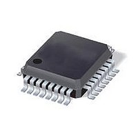
Manufacturer Part Number
ST7FLI49MK1T6
Description
MCU 8BIT SGL VOLT FLASH 32-LQFP
Manufacturer
STMicroelectronics
Series
ST7r
Datasheet
1.ST7FLI49MK1T6TR.pdf
(187 pages)
Specifications of ST7FLI49MK1T6
Core Processor
ST7
Core Size
8-Bit
Speed
8MHz
Connectivity
I²C
Peripherals
LVD, POR, PWM, WDT
Number Of I /o
24
Program Memory Size
4KB (4K x 8)
Program Memory Type
FLASH
Eeprom Size
128 x 8
Ram Size
384 x 8
Voltage - Supply (vcc/vdd)
2.4 V ~ 5.5 V
Data Converters
A/D 10x10b
Oscillator Type
Internal
Operating Temperature
-40°C ~ 85°C
Package / Case
32-LQFP
Processor Series
ST7FLI4x
Core
ST7
Data Bus Width
8 bit
Data Ram Size
384 B
Interface Type
I2C
Maximum Clock Frequency
8 MHz
Number Of Programmable I/os
24
Number Of Timers
5
Maximum Operating Temperature
+ 125 C
Mounting Style
SMD/SMT
Minimum Operating Temperature
- 40 C
On-chip Adc
10 bit, 10 Channel
Lead Free Status / RoHS Status
Lead free / RoHS Compliant
Available stocks
Company
Part Number
Manufacturer
Quantity
Price
Company:

Part Number:
ST7FLI49MK1T6
Manufacturer:
st
Quantity:
456
Company:
Part Number:
ST7FLI49MK1T6
Manufacturer:
STMicroelectronics
Quantity:
10 000
Part Number:
ST7FLI49MK1T6
Manufacturer:
ST
Quantity:
20 000
Company:
Part Number:
ST7FLI49MK1T6TR
Manufacturer:
STMicroelectronics
Quantity:
10 000


I/O ports
10.2.3
Caution:
70/188
Alternate functions
Many ST7s I/Os have one or more alternate functions. These may include output signals
from, or input signals to, on-chip
be input/output to which ports.
A signal coming from an on-chip peripheral can be output on an I/O. To do this, enable the
on-chip peripheral as an output (enable bit in the peripheral’s control register). The
peripheral configures the I/O as an output and takes priority over standard I/O programming.
The I/O’s state is readable by addressing the corresponding I/O data register.
Configuring an I/O as floating enables alternate function input. It is not recommended to
configure an I/O as pull-up as this will increase current consumption. Before using an I/O as
an alternate input, configure it without interrupt. Otherwise spurious interrupts can occur.
Configure an I/O as input floating for an on-chip peripheral signal which can be input and
output.
I/Os which can be configured as both an analog and digital alternate function need special
attention. The user must control the peripherals so that the signals do not arrive at the same
time on the same pin. If an external clock is used, only the clock alternate function should be
employed on that I/O pin and not the other alternate function.
Figure 34. I/O port general block diagram
REGISTER
ACCESS
EXTERNAL
INTERRUPT
REQUEST (ei
DDR SEL
OR SEL
DR SEL
DDR
OR
DR
x
)
SENSITIVITY
SELECTION
ALTERNATE
OUTPUT
From on-chip periphera
ALTERNATE
ENABLE
BIT
If implemented
1
0
Combinational
Logic
Doc ID 13562 Rev 3
l
peripherals.Table 2
1
0
FROM
OTHER
BITS
Note: Refer to the Port Configuration
table for device specific information.
N-BUFFER
PULL-UP
CONDITION
describes which peripheral signals can
SCHMITT
TRIGGER
CMOS
V
DD
P-BUFFER
(see table below)
To on-chip peripheral
V
DD
DIODES
(see table below)
PULL-UP
(see table below)
ALTERNATE
ANALOG
INPUT
INPUT
PAD
ST7LITE49M
Related parts for ST7FLI49MK1T6
Image
Part Number
Description
Manufacturer
Datasheet
Request
R

Part Number:
Description:
BOARD DAUGHTER 32LQFP ST7FLITE4
Manufacturer:
STMicroelectronics
Datasheet:
Part Number:
Description:
STMicroelectronics [RIPPLE-CARRY BINARY COUNTER/DIVIDERS]
Manufacturer:
STMicroelectronics
Datasheet:
Part Number:
Description:
STMicroelectronics [LIQUID-CRYSTAL DISPLAY DRIVERS]
Manufacturer:
STMicroelectronics
Datasheet:

Part Number:
Description:
BOARD EVAL FOR MEMS SENSORS
Manufacturer:
STMicroelectronics
Datasheet:
Part Number:
Description:
NPN TRANSISTOR POWER MODULE
Manufacturer:
STMicroelectronics
Datasheet:
Part Number:
Description:
TURBOSWITCH ULTRA-FAST HIGH VOLTAGE DIODE
Manufacturer:
STMicroelectronics
Datasheet:
Part Number:
Description:
Manufacturer:
STMicroelectronics
Datasheet:
Part Number:
Description:
DIODE / SCR MODULE
Manufacturer:
STMicroelectronics
Datasheet:
Part Number:
Description:
DIODE / SCR MODULE
Manufacturer:
STMicroelectronics
Datasheet:
Part Number:
Description:
Search -----> STE16N100
Manufacturer:
STMicroelectronics
Datasheet:
Part Number:
Description:
Search ---> STE53NA50
Manufacturer:
STMicroelectronics
Datasheet:
Part Number:
Description:
NPN Transistor Power Module
Manufacturer:
STMicroelectronics
Datasheet: