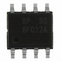
Z8F012ASB020SG Zilog, Z8F012ASB020SG Datasheet - Page 180

Z8F012ASB020SG
Manufacturer Part Number
Z8F012ASB020SG
Description
IC ENCORE XP MCU FLASH 1K 8SOIC
Manufacturer
Zilog
Series
Encore!® XP®r
Datasheet
1.Z8F011ASB020EG.pdf
(282 pages)
Specifications of Z8F012ASB020SG
Core Processor
Z8
Core Size
8-Bit
Speed
20MHz
Connectivity
IrDA, UART/USART
Peripherals
Brown-out Detect/Reset, LED, LVD, POR, PWM, Temp Sensor, WDT
Number Of I /o
6
Program Memory Size
1KB (1K x 8)
Program Memory Type
FLASH
Eeprom Size
16 x 8
Ram Size
256 x 8
Voltage - Supply (vcc/vdd)
2.7 V ~ 3.6 V
Data Converters
A/D 4x10b
Oscillator Type
Internal
Operating Temperature
0°C ~ 70°C
Package / Case
8-SOIC (3.9mm Width)
Processor Series
Z8F012Ax
Core
eZ8
Data Bus Width
8 bit
Data Ram Size
256 B
Interface Type
UART
Maximum Clock Frequency
20 MHz
Number Of Programmable I/os
6
Number Of Timers
2
Operating Supply Voltage
2.7 V to 3.6 V
Maximum Operating Temperature
+ 70 C
Mounting Style
SMD/SMT
Development Tools By Supplier
Z8F04A08100KITG, Z8F04A28100KITG, ZENETSC0100ZACG, ZENETSC0100ZACG, ZUSBOPTSC01ZACG, ZUSBSC00100ZAC, ZUSBSC00100ZACG
Minimum Operating Temperature
0 C
On-chip Adc
10 bit, 4 Channel
Lead Free Status / RoHS Status
Lead free / RoHS Compliant
Other names
269-4039
Z8F012ASB020SG
Z8F012ASB020SG
- Current page: 180 of 282
- Download datasheet (4Mb)
Non-Volatile Data Storage
Operation
NVDS Code Interface
PS022825-0908
Note:
Byte Write
The Z8 Encore! XP
element of up to 128 bytes. This memory can perform over 100,000 write cycles.
The NVDS is implemented by special purpose Zilog
memory, which are not user-accessible. These special-purpose routines use the Flash
memory to store the data. The routines incorporate a dynamic addressing scheme to
maximize the write/erase endurance of the Flash.
Different members of the Z8 Encore! XP F082A Series feature multiple NVDS array sizes.
See
Also the members containing 8 KB of Flash memory do not include the NVDS feature.
Two routines are required to access the NVDS: a write routine and a read routine. Both of
these routines are accessed with a CALL instruction to a pre-defined address outside of the
user-accessible program memory. Both the NVDS address and data are single-byte values.
Because these routines disturb the working register set, user code must ensure that any
required working register values are preserved by pushing them onto the stack or by
changing the working register pointer just prior to NVDS execution.
During both read and write accesses to the NVDS, interrupt service is NOT disabled. Any
interrupts that occur during the NVDS execution must take care not to disturb the working
register and existing stack contents or else the array may become corrupted. Disabling
interrupts before executing NVDS operations is recommended.
Use of the NVDS requires 15 bytes of available stack space. Also, the contents of the
working register set are overwritten.
For correct NVDS operation, the Flash Frequency Registers must be programmed based
on the system clock frequency (see
Registers
To write a byte to the NVDS array, the user code must first push the address, then the data
byte onto the stack. The user code issues a
byte-write routine (0x10B3). At the return from the sub-routine, the write status byte
Z8 Encore! XP
on page 145
®
®
F082A Series devices contain a non-volatile data storage (NVDS)
).
F082A Series Family Part Selection Guide
Flash Operation Timing Using the Flash Frequency
CALL
instruction to the address of the
®
software stored in areas of program
Z8 Encore! XP
Product Specification
Non-Volatile Data Storage
on page 3 for details.
®
F082A Series
169
Related parts for Z8F012ASB020SG
Image
Part Number
Description
Manufacturer
Datasheet
Request
R

Part Number:
Description:
Communication Controllers, ZILOG INTELLIGENT PERIPHERAL CONTROLLER (ZIP)
Manufacturer:
Zilog, Inc.
Datasheet:

Part Number:
Description:
KIT DEV FOR Z8 ENCORE 16K TO 64K
Manufacturer:
Zilog
Datasheet:

Part Number:
Description:
KIT DEV Z8 ENCORE XP 28-PIN
Manufacturer:
Zilog
Datasheet:

Part Number:
Description:
DEV KIT FOR Z8 ENCORE 8K/4K
Manufacturer:
Zilog
Datasheet:

Part Number:
Description:
KIT DEV Z8 ENCORE XP 28-PIN
Manufacturer:
Zilog
Datasheet:

Part Number:
Description:
DEV KIT FOR Z8 ENCORE 4K TO 8K
Manufacturer:
Zilog
Datasheet:

Part Number:
Description:
CMOS Z8 microcontroller. ROM 16 Kbytes, RAM 256 bytes, speed 16 MHz, 32 lines I/O, 3.0V to 5.5V
Manufacturer:
Zilog, Inc.
Datasheet:

Part Number:
Description:
Low-cost microcontroller. 512 bytes ROM, 61 bytes RAM, 8 MHz
Manufacturer:
Zilog, Inc.
Datasheet:

Part Number:
Description:
Z8 4K OTP Microcontroller
Manufacturer:
Zilog, Inc.
Datasheet:

Part Number:
Description:
CMOS SUPER8 ROMLESS MCU
Manufacturer:
Zilog, Inc.
Datasheet:

Part Number:
Description:
SL1866 CMOSZ8 OTP Microcontroller
Manufacturer:
Zilog, Inc.
Datasheet:

Part Number:
Description:
SL1866 CMOSZ8 OTP Microcontroller
Manufacturer:
Zilog, Inc.
Datasheet:

Part Number:
Description:
OTP (KB) = 1, RAM = 125, Speed = 12, I/O = 14, 8-bit Timers = 2, Comm Interfaces Other Features = Por, LV Protect, Voltage = 4.5-5.5V
Manufacturer:
Zilog, Inc.
Datasheet:

Part Number:
Description:
Manufacturer:
Zilog, Inc.
Datasheet:


