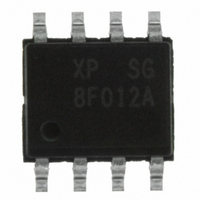
Z8F012ASB020SG Zilog, Z8F012ASB020SG Datasheet - Page 35
Z8F012ASB020SG
Manufacturer Part Number
Z8F012ASB020SG
Description
IC ENCORE XP MCU FLASH 1K 8SOIC
Manufacturer
Zilog
Series
Encore!® XP®r
Datasheet
1.Z8F011ASB020EG.pdf
(282 pages)
Specifications of Z8F012ASB020SG
Core Processor
Z8
Core Size
8-Bit
Speed
20MHz
Connectivity
IrDA, UART/USART
Peripherals
Brown-out Detect/Reset, LED, LVD, POR, PWM, Temp Sensor, WDT
Number Of I /o
6
Program Memory Size
1KB (1K x 8)
Program Memory Type
FLASH
Eeprom Size
16 x 8
Ram Size
256 x 8
Voltage - Supply (vcc/vdd)
2.7 V ~ 3.6 V
Data Converters
A/D 4x10b
Oscillator Type
Internal
Operating Temperature
0°C ~ 70°C
Package / Case
8-SOIC (3.9mm Width)
Processor Series
Z8F012Ax
Core
eZ8
Data Bus Width
8 bit
Data Ram Size
256 B
Interface Type
UART
Maximum Clock Frequency
20 MHz
Number Of Programmable I/os
6
Number Of Timers
2
Operating Supply Voltage
2.7 V to 3.6 V
Maximum Operating Temperature
+ 70 C
Mounting Style
SMD/SMT
Development Tools By Supplier
Z8F04A08100KITG, Z8F04A28100KITG, ZENETSC0100ZACG, ZENETSC0100ZACG, ZUSBOPTSC01ZACG, ZUSBSC00100ZAC, ZUSBSC00100ZACG
Minimum Operating Temperature
0 C
On-chip Adc
10 bit, 4 Channel
Lead Free Status / RoHS Status
Lead free / RoHS Compliant
Other names
269-4039
Z8F012ASB020SG
Z8F012ASB020SG


Table 8. Reset and Stop Mode Recovery Characteristics and Latency
PS022825-0908
Reset Type
System Reset
System Reset with Crystal
Oscillator Enabled
Stop Mode Recovery
Stop Mode Recovery with
Crystal Oscillator Enabled
During a System Reset or Stop Mode Recovery, the Internal Precision Oscillator requires
4
cycles of the Internal Precision Oscillator. If the crystal oscillator is enabled in the Flash
option bits, this reset period is increased to 5000 IPO cycles. When a reset occurs because
of a low voltage condition or Power-On Reset (POR), this delay is measured from the time
that the supply voltage first exceeds the POR level. If the external pin reset remains
asserted at the end of the reset period, the device remains in reset until the pin is deas-
serted.
At the beginning of Reset, all GPIO pins are configured as inputs with pull-up resistor dis-
abled, except PD0 (or PA2 on 8-pin devices) which is shared with the reset pin. On reset,
the PD0 is configured as a bidirectional open-drain reset. The pin is internally driven low
during port reset, after which the user code may reconfigure this pin as a general purpose
output.
During Reset, the eZ8 CPU and on-chip peripherals are idle; however, the on-chip crystal
oscillator and Watchdog Timer oscillator continue to run.
Upon Reset, control registers within the Register File that have a defined Reset value are
loaded with their reset values. Other control registers (including the Stack Pointer,
Register Pointer, and Flags) and general-purpose RAM are undefined following Reset.
The eZ8 CPU fetches the Reset vector at Program Memory addresses
and loads that value into the Program Counter. Program execution begins at the Reset
vector address.
As the control registers are re-initialized by a system reset, the system clock after reset is
always the IPO. The software must reconfigure the oscillator control block, such that the
correct system clock source is enabled and selected.
µ
s to start up. Then the Z8 Encore! XP F082A Series device is held in Reset for 66
Control Registers
Reset (as applicable)
Reset (as applicable)
Unaffected, except
WDT_CTL and
OSC_CTL registers
Unaffected, except
WDT_CTL and
OSC_CTL registers
Reset Characteristics and Latency
Reset 66 Internal Precision Oscillator Cycles
Reset 5000 Internal Precision Oscillator Cycles
Reset 66 Internal Precision Oscillator Cycles
Reset 5000 Internal Precision Oscillator Cycles
Reset, Stop Mode Recovery, and Low Voltage Detection
CPU
eZ8
Reset Latency (Delay)
+ IPO startup time
Z8 Encore! XP
Product Specification
0002H
®
F082A Series
and
0003H
24
Related parts for Z8F012ASB020SG
Image
Part Number
Description
Manufacturer
Datasheet
Request
R

Part Number:
Description:
Communication Controllers, ZILOG INTELLIGENT PERIPHERAL CONTROLLER (ZIP)
Manufacturer:
Zilog, Inc.
Datasheet:

Part Number:
Description:
KIT DEV FOR Z8 ENCORE 16K TO 64K
Manufacturer:
Zilog
Datasheet:

Part Number:
Description:
KIT DEV Z8 ENCORE XP 28-PIN
Manufacturer:
Zilog
Datasheet:

Part Number:
Description:
DEV KIT FOR Z8 ENCORE 8K/4K
Manufacturer:
Zilog
Datasheet:

Part Number:
Description:
KIT DEV Z8 ENCORE XP 28-PIN
Manufacturer:
Zilog
Datasheet:

Part Number:
Description:
DEV KIT FOR Z8 ENCORE 4K TO 8K
Manufacturer:
Zilog
Datasheet:
Part Number:
Description:
CMOS Z8 microcontroller. ROM 16 Kbytes, RAM 256 bytes, speed 16 MHz, 32 lines I/O, 3.0V to 5.5V
Manufacturer:
Zilog, Inc.
Datasheet:
Part Number:
Description:
Low-cost microcontroller. 512 bytes ROM, 61 bytes RAM, 8 MHz
Manufacturer:
Zilog, Inc.
Datasheet:
Part Number:
Description:
Z8 4K OTP Microcontroller
Manufacturer:
Zilog, Inc.
Datasheet:
Part Number:
Description:
CMOS SUPER8 ROMLESS MCU
Manufacturer:
Zilog, Inc.
Datasheet:
Part Number:
Description:
SL1866 CMOSZ8 OTP Microcontroller
Manufacturer:
Zilog, Inc.
Datasheet:
Part Number:
Description:
SL1866 CMOSZ8 OTP Microcontroller
Manufacturer:
Zilog, Inc.
Datasheet:
Part Number:
Description:
OTP (KB) = 1, RAM = 125, Speed = 12, I/O = 14, 8-bit Timers = 2, Comm Interfaces Other Features = Por, LV Protect, Voltage = 4.5-5.5V
Manufacturer:
Zilog, Inc.
Datasheet:
Part Number:
Description:
Manufacturer:
Zilog, Inc.
Datasheet: