R5F21356CNFP#U0 Renesas Electronics America, R5F21356CNFP#U0 Datasheet - Page 170
R5F21356CNFP#U0
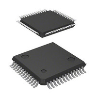
Manufacturer Part Number
R5F21356CNFP#U0
Description
MCU 1KB FLASH 32K ROM 52-LQFP
Manufacturer
Renesas Electronics America
Series
R8C/3x/35Cr
Datasheet
1.R5F21356CNFPU0.pdf
(762 pages)
Specifications of R5F21356CNFP#U0
Core Processor
R8C
Core Size
16/32-Bit
Speed
20MHz
Connectivity
I²C, LIN, SIO, SSU, UART/USART
Peripherals
POR, PWM, Voltage Detect, WDT
Number Of I /o
47
Program Memory Size
32KB (32K x 8)
Program Memory Type
FLASH
Ram Size
2.5K x 8
Voltage - Supply (vcc/vdd)
1.8 V ~ 5.5 V
Data Converters
A/D 12x10b; D/A 2x8b
Oscillator Type
Internal
Operating Temperature
-20°C ~ 85°C
Package / Case
52-LQFP
Lead Free Status / RoHS Status
Lead free / RoHS Compliant
Eeprom Size
-
Available stocks
Company
Part Number
Manufacturer
Quantity
Price


R8C/35C Group
REJ09B0567-0100 Rev.1.00 Dec. 14, 2009
Page 137 of 725
9.7.2
9.7.2.1
9.7.2.2
9.7.2.3
Since the CPU clock stops in wait mode, the CPU operating with the CPU clock and the watchdog timer when
count source protection mode is disabled stop. Since the XIN clock, XCIN clock, and on-chip oscillator clock
do not stop, the peripheral functions using these clocks continue operating.
If the CM02 bit is set to 1 (peripheral function clock stops in wait mode), the f1, f2, f4, f8, and f32 clocks stop
in wait mode. This reduces power consumption.
The MCU enters wait mode by executing the WAIT instruction or setting the CM30 bit in the CM3 register to 1
(MCU enters wait mode).
When the OCD2 bit in the OCD register is set to 1 (on-chip oscillator selected as system clock), set the OCD1
bit in the OCD register to 0 (oscillation stop detection interrupt disabled) before executing the WAIT
instruction or setting the CM30 bit in the CM3 register to 1(MCU enters wait mode).
If the MCU enters wait mode while the OCD1 bit is set to 1 (oscillation stop detection interrupt enabled),
current consumption is not reduced because the CPU clock does not stop.
Enter wait mode after setting the FMR27 bit to 0 (low-current-consumption read mode disabled). Do not enter
wait mode while the FMR27 bit is 1 (low-current-consumption read mode enabled).
The I/O port retains the status immediately before the MCU enters wait mode.
Wait Mode
Peripheral Function Clock Stop Function
Entering Wait Mode
Pin Status in Wait Mode
9. Clock Generation Circuit
Related parts for R5F21356CNFP#U0
Image
Part Number
Description
Manufacturer
Datasheet
Request
R

Part Number:
Description:
KIT STARTER FOR M16C/29
Manufacturer:
Renesas Electronics America
Datasheet:

Part Number:
Description:
KIT STARTER FOR R8C/2D
Manufacturer:
Renesas Electronics America
Datasheet:

Part Number:
Description:
R0K33062P STARTER KIT
Manufacturer:
Renesas Electronics America
Datasheet:

Part Number:
Description:
KIT STARTER FOR R8C/23 E8A
Manufacturer:
Renesas Electronics America
Datasheet:

Part Number:
Description:
KIT STARTER FOR R8C/25
Manufacturer:
Renesas Electronics America
Datasheet:

Part Number:
Description:
KIT STARTER H8S2456 SHARPE DSPLY
Manufacturer:
Renesas Electronics America
Datasheet:

Part Number:
Description:
KIT STARTER FOR R8C38C
Manufacturer:
Renesas Electronics America
Datasheet:

Part Number:
Description:
KIT STARTER FOR R8C35C
Manufacturer:
Renesas Electronics America
Datasheet:

Part Number:
Description:
KIT STARTER FOR R8CL3AC+LCD APPS
Manufacturer:
Renesas Electronics America
Datasheet:
Part Number:
Description:
KIT STARTER FOR RX610
Manufacturer:
Renesas Electronics America
Datasheet:

Part Number:
Description:
KIT STARTER FOR R32C/118
Manufacturer:
Renesas Electronics America
Datasheet:

Part Number:
Description:
KIT DEV RSK-R8C/26-29
Manufacturer:
Renesas Electronics America
Datasheet:

Part Number:
Description:
KIT STARTER FOR SH7124
Manufacturer:
Renesas Electronics America
Datasheet:

Part Number:
Description:
KIT STARTER FOR H8SX/1622
Manufacturer:
Renesas Electronics America
Datasheet:

Part Number:
Description:
KIT DEV FOR SH7203
Manufacturer:
Renesas Electronics America
Datasheet: