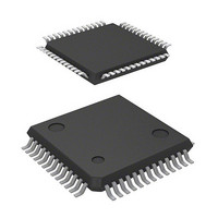
R5F21356CNFP#U0 Renesas Electronics America, R5F21356CNFP#U0 Datasheet - Page 675

R5F21356CNFP#U0
Manufacturer Part Number
R5F21356CNFP#U0
Description
MCU 1KB FLASH 32K ROM 52-LQFP
Manufacturer
Renesas Electronics America
Series
R8C/3x/35Cr
Datasheet
1.R5F21356CNFPU0.pdf
(762 pages)
Specifications of R5F21356CNFP#U0
Core Processor
R8C
Core Size
16/32-Bit
Speed
20MHz
Connectivity
I²C, LIN, SIO, SSU, UART/USART
Peripherals
POR, PWM, Voltage Detect, WDT
Number Of I /o
47
Program Memory Size
32KB (32K x 8)
Program Memory Type
FLASH
Ram Size
2.5K x 8
Voltage - Supply (vcc/vdd)
1.8 V ~ 5.5 V
Data Converters
A/D 12x10b; D/A 2x8b
Oscillator Type
Internal
Operating Temperature
-20°C ~ 85°C
Package / Case
52-LQFP
Lead Free Status / RoHS Status
Lead free / RoHS Compliant
Eeprom Size
-
Available stocks
Company
Part Number
Manufacturer
Quantity
Price
- Current page: 675 of 762
- Download datasheet (8Mb)
R8C/35C Group
REJ09B0567-0100 Rev.1.00 Dec. 14, 2009
Page 642 of 725
31.4.11.4 Block Erase Command
When 20h is written in the first bus cycle and then D0h is written in the second bus cycle to any block address,
auto-erasure (erase and erase verify operation) starts in the specified block.
The FST7 bit in the FST register can be used to confirm whether auto-erasure has completed. The FST7 bit is
set to 0 during auto-erasure and is set to 1 when auto-erasure completes. After auto-erasure completes, all data
in the block is set to FFh.
After auto-erasure has completed, the auto-erase result can be confirmed by the FST5 bit in the FST register.
(Refer to 31.4.12 Full Status Check).
The block erase command targeting each block in the program ROM can be disabled using the lock bit.
The following commands are not accepted under the following conditions:
•
•
•
•
Figure 31.11 shows a Block Erase Flowchart (Flash Ready Status Interrupt Disabled), Figure 31.12 shows a
Block Erase Flowchart (Flash Ready Status Interrupt Disabled and Suspend Enabled), and Figure 31.13 shows
a Block Erase Flowchart (Flash Ready Status Interrupt Enabled and Suspend Enabled).
In EW1 mode, do not execute this command to any block where a rewrite control program is allocated.
While the RDYSTIE bit in the FMR0 register is set to 1 (flash ready status interrupt enabled), a flash ready
status interrupt can be generated upon completion of auto-erasure. While the RDYSTIE bit is set to 1 and the
FMR20 bit in the FMR2 register is set to 1 (erase-suspend enabled), a flash ready status interrupt is generated
when the FMR21 bit is set to 1 (erase-suspend request) and auto-erasure suspends. The auto-erase result can be
confirmed by reading the FST register during the interrupt routine.
Block erase commands targeting data flash block A when the FMR14 bit in the FMR1 register is set to 1
(rewrite disabled).
Block erase commands targeting data flash block B when the FMR15 bit is set to 1 (rewrite disabled).
Block erase commands targeting data flash block C when the FMR16 bit is set to 1 (rewrite disabled).
Block erase commands targeting data flash block D when the FMR17 bit is set to 1 (rewrite disabled).
31. Flash Memory
Related parts for R5F21356CNFP#U0
Image
Part Number
Description
Manufacturer
Datasheet
Request
R

Part Number:
Description:
KIT STARTER FOR M16C/29
Manufacturer:
Renesas Electronics America
Datasheet:

Part Number:
Description:
KIT STARTER FOR R8C/2D
Manufacturer:
Renesas Electronics America
Datasheet:

Part Number:
Description:
R0K33062P STARTER KIT
Manufacturer:
Renesas Electronics America
Datasheet:

Part Number:
Description:
KIT STARTER FOR R8C/23 E8A
Manufacturer:
Renesas Electronics America
Datasheet:

Part Number:
Description:
KIT STARTER FOR R8C/25
Manufacturer:
Renesas Electronics America
Datasheet:

Part Number:
Description:
KIT STARTER H8S2456 SHARPE DSPLY
Manufacturer:
Renesas Electronics America
Datasheet:

Part Number:
Description:
KIT STARTER FOR R8C38C
Manufacturer:
Renesas Electronics America
Datasheet:

Part Number:
Description:
KIT STARTER FOR R8C35C
Manufacturer:
Renesas Electronics America
Datasheet:

Part Number:
Description:
KIT STARTER FOR R8CL3AC+LCD APPS
Manufacturer:
Renesas Electronics America
Datasheet:

Part Number:
Description:
KIT STARTER FOR RX610
Manufacturer:
Renesas Electronics America
Datasheet:

Part Number:
Description:
KIT STARTER FOR R32C/118
Manufacturer:
Renesas Electronics America
Datasheet:

Part Number:
Description:
KIT DEV RSK-R8C/26-29
Manufacturer:
Renesas Electronics America
Datasheet:

Part Number:
Description:
KIT STARTER FOR SH7124
Manufacturer:
Renesas Electronics America
Datasheet:

Part Number:
Description:
KIT STARTER FOR H8SX/1622
Manufacturer:
Renesas Electronics America
Datasheet:

Part Number:
Description:
KIT DEV FOR SH7203
Manufacturer:
Renesas Electronics America
Datasheet:


