R5F21356CNFP#U0 Renesas Electronics America, R5F21356CNFP#U0 Datasheet - Page 736
R5F21356CNFP#U0
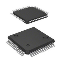
Manufacturer Part Number
R5F21356CNFP#U0
Description
MCU 1KB FLASH 32K ROM 52-LQFP
Manufacturer
Renesas Electronics America
Series
R8C/3x/35Cr
Datasheet
1.R5F21356CNFPU0.pdf
(762 pages)
Specifications of R5F21356CNFP#U0
Core Processor
R8C
Core Size
16/32-Bit
Speed
20MHz
Connectivity
I²C, LIN, SIO, SSU, UART/USART
Peripherals
POR, PWM, Voltage Detect, WDT
Number Of I /o
47
Program Memory Size
32KB (32K x 8)
Program Memory Type
FLASH
Ram Size
2.5K x 8
Voltage - Supply (vcc/vdd)
1.8 V ~ 5.5 V
Data Converters
A/D 12x10b; D/A 2x8b
Oscillator Type
Internal
Operating Temperature
-20°C ~ 85°C
Package / Case
52-LQFP
Lead Free Status / RoHS Status
Lead free / RoHS Compliant
Eeprom Size
-
Available stocks
Company
Part Number
Manufacturer
Quantity
Price


R8C/35C Group
REJ09B0567-0100 Rev.1.00 Dec. 14, 2009
Page 703 of 725
34.9.5
34.9.6
34.9.7
•
Switching procedure
(1) Set the TSTARTi (i = 0 or 1) bit in the TRDSTR register to 0 (count stops).
(2) Change bits TCK2 to TCK0 in the TRDCRi register.
•
Switching procedure
(1) Set the TSTARTi (i = 0 or 1) bit in the TRDSTR register to 0 (count stops).
(2) Change bits TCK2 to TCK0 in the TRDCRi register.
(3) Wait 2 or more cycles of f1.
(4) Set the FRA00 bit in the FRA0 register to 0 (high-speed on-chip oscillator stops).
•
Switching procedure
(1) Set the TSTARTi (i = 0 to 1) bit in the TRDSTR register to 0 (count stops).
(2) Change the settings of bits TCK2 to TCK0 in the TRDCRi register.
(3) Wait for a minimum of two cycles of fOCO-F.
(4) Set the FRA00 bit in the FRA0 register to 0 (high-speed on-chip oscillator off).
•
Switching procedure
(1) Set the TSTARTi (i = 0 to 1) bit in the TRDSTR register to 0 (count stops).
(2) Change the settings of bits TCK2 to TCK0 in the TRDCRi register.
(3) Wait for a minimum of one cycle of fOCO-F + fOCO40M.
(4) Set the FRA00 bit in the FRA0 register to 0 (high-speed on-chip oscillator off).
•
•
•
•
Switching procedure
(1) Set the TSTART0 bit in the TRDSTR register to 0 (count stops).
(2) Set bits CMD1 to CMD0 in the TRDFCR register to 00b (timer mode, PWM mode, and PWM3 mode).
(3) Set bits CMD1 to CMD0 to 01b (reset synchronous PWM mode).
(4) Set the other registers associated with timer RD again.
Switch the count source after the count stops.
When changing the count source from fOCO40M to another source and stopping fOCO40M, wait 2 cycles of
f1 or more after setting the clock switch, and then stop fOCO40M.
After switching the count source from fOCO-F to fOCO40M, allow a minimum of two cycles of fOCO-F to
elapse after changing the clock setting before stopping fOCO-F.
After switching the count source from fOCO-F to a clock other than fOCO40M, allow a minimum of one
cycle of fOCO-F + fOCO40M to elapse after changing the clock setting before stopping fOCO-F.
Set the pulse width of the input capture signal to 3 or more cycles of the timer RD operation clock (refer to
Table 20.1 Timer RD Operation Clocks).
The value in the TRDi register is transferred to the TRDGRji register 2 to 3 cycles of the timer RD operation
clock after the input capture signal is applied to the TRDIOji pin (i = 0 or 1, j = A, B, C, or D) (no digital
filter).
When reset synchronous PWM mode is used for motor control, make sure OLS0 = OLS1.
Set to reset synchronous PWM mode by the following procedure:
Count Source Switch
Input Capture Function
Reset Synchronous PWM Mode
34. Usage Notes
Related parts for R5F21356CNFP#U0
Image
Part Number
Description
Manufacturer
Datasheet
Request
R

Part Number:
Description:
KIT STARTER FOR M16C/29
Manufacturer:
Renesas Electronics America
Datasheet:

Part Number:
Description:
KIT STARTER FOR R8C/2D
Manufacturer:
Renesas Electronics America
Datasheet:

Part Number:
Description:
R0K33062P STARTER KIT
Manufacturer:
Renesas Electronics America
Datasheet:

Part Number:
Description:
KIT STARTER FOR R8C/23 E8A
Manufacturer:
Renesas Electronics America
Datasheet:

Part Number:
Description:
KIT STARTER FOR R8C/25
Manufacturer:
Renesas Electronics America
Datasheet:

Part Number:
Description:
KIT STARTER H8S2456 SHARPE DSPLY
Manufacturer:
Renesas Electronics America
Datasheet:

Part Number:
Description:
KIT STARTER FOR R8C38C
Manufacturer:
Renesas Electronics America
Datasheet:

Part Number:
Description:
KIT STARTER FOR R8C35C
Manufacturer:
Renesas Electronics America
Datasheet:

Part Number:
Description:
KIT STARTER FOR R8CL3AC+LCD APPS
Manufacturer:
Renesas Electronics America
Datasheet:
Part Number:
Description:
KIT STARTER FOR RX610
Manufacturer:
Renesas Electronics America
Datasheet:

Part Number:
Description:
KIT STARTER FOR R32C/118
Manufacturer:
Renesas Electronics America
Datasheet:

Part Number:
Description:
KIT DEV RSK-R8C/26-29
Manufacturer:
Renesas Electronics America
Datasheet:

Part Number:
Description:
KIT STARTER FOR SH7124
Manufacturer:
Renesas Electronics America
Datasheet:

Part Number:
Description:
KIT STARTER FOR H8SX/1622
Manufacturer:
Renesas Electronics America
Datasheet:

Part Number:
Description:
KIT DEV FOR SH7203
Manufacturer:
Renesas Electronics America
Datasheet: