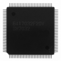
HD6417032F20V Renesas Electronics America, HD6417032F20V Datasheet - Page 268

HD6417032F20V
Manufacturer Part Number
HD6417032F20V
Description
SH1 ROMLESS LEAD FREE
Manufacturer
Renesas Electronics America
Series
SuperH® SH7030r
Datasheet
1.HD6417034AFI20.pdf
(689 pages)
Specifications of HD6417032F20V
Core Processor
SH-1
Core Size
32-Bit
Speed
20MHz
Connectivity
EBI/EMI, SCI
Peripherals
DMA, POR, PWM, WDT
Number Of I /o
32
Program Memory Type
ROMless
Ram Size
4K x 8
Voltage - Supply (vcc/vdd)
4.5 V ~ 5.5 V
Data Converters
A/D 8x10b
Oscillator Type
Internal
Operating Temperature
-20°C ~ 75°C
Package / Case
112-QFP
Lead Free Status / RoHS Status
Lead free / RoHS Compliant
Eeprom Size
-
Program Memory Size
-
Available stocks
Company
Part Number
Manufacturer
Quantity
Price
Company:
Part Number:
HD6417032F20V
Manufacturer:
TI
Quantity:
201
- Current page: 268 of 689
- Download datasheet (5Mb)
Section 10 16-Bit Integrated Timer Pulse Unit (ITU)
Bits 7 and 6—Reserved: Bit 7 is read as undefined. Bit 6 is always read as 1. The write value to
bit 7 should be 0 or 1. The write value to bit 6 should always be 1.
Bits 5 and 4—Combination Mode 1 and 0 (CMD1 and CMD0): CMD1 and CMD0 select
complementary PWM mode or reset-synchronized mode for channels 3 and 4. Set the
complementary PWM/reset-synchronized PWM mode while the timer counter (TCNT) being used
is off. When these bits are used to set complementary PWM/reset-synchronized PWM mode, they
take priority over the PWM4 and PWM3 bits in TMDR. While the complementary PWM/reset-
synchronized PWM mode settings and the SYNC4 and SYNC3 bit settings of the timer synchro
register (TSNC) are valid simultaneously, when complementary PWM mode is set, channels 3 and
4 should not be set to operate simultaneously (the SYNC 4 and SYNC 3 bits in TSNC should not
both be set to 1).
Bit 5: CMD1
0
1
Bit 3—Buffer Mode B4 (BFB4): BFB4 selects buffer mode for GRB4 and BRB4 in channel 4.
Bit 3: BFB4
0
1
Bit 2—Buffer Mode A4 (BFA4): BFA4 selects buffer mode for GRA4 and BRA4 in channel 4.
Bit 2: BFA4
0
1
Bit 1—Buffer Mode B3 (BFB3): BFB3 selects buffer mode for GRB3 and BRB3 in channel 3.
Bit 1: BFB3
0
1
Rev. 7.00 Jan 31, 2006 page 240 of 658
REJ09B0272-0700
Bit 4: CMD0 Description
0
1
0
1
Description
GRB4 operates normally in channel 4
GRB4 and BRB4 operate in buffer mode in channel 4
Description
GRA4 operates normally in channel 4
GRA4 and BRA4 operate in buffer mode in channel 4
Description
GRB3 operates normally in channel 3
GRB3 and BRB3 operate in buffer mode in channel 3
Channels 3 and 4 operate normally
Channels 3 and 4 operate normally
Channels 3 and 4 operate together in complementary PWM mode
Channels 3 and 4 operate together in reset-synchronized PWM
mode
(Initial value)
(Initial value)
(Initial value)
(Initial value)
Related parts for HD6417032F20V
Image
Part Number
Description
Manufacturer
Datasheet
Request
R

Part Number:
Description:
KIT STARTER FOR M16C/29
Manufacturer:
Renesas Electronics America
Datasheet:

Part Number:
Description:
KIT STARTER FOR R8C/2D
Manufacturer:
Renesas Electronics America
Datasheet:

Part Number:
Description:
R0K33062P STARTER KIT
Manufacturer:
Renesas Electronics America
Datasheet:

Part Number:
Description:
KIT STARTER FOR R8C/23 E8A
Manufacturer:
Renesas Electronics America
Datasheet:

Part Number:
Description:
KIT STARTER FOR R8C/25
Manufacturer:
Renesas Electronics America
Datasheet:

Part Number:
Description:
KIT STARTER H8S2456 SHARPE DSPLY
Manufacturer:
Renesas Electronics America
Datasheet:

Part Number:
Description:
KIT STARTER FOR R8C38C
Manufacturer:
Renesas Electronics America
Datasheet:

Part Number:
Description:
KIT STARTER FOR R8C35C
Manufacturer:
Renesas Electronics America
Datasheet:

Part Number:
Description:
KIT STARTER FOR R8CL3AC+LCD APPS
Manufacturer:
Renesas Electronics America
Datasheet:

Part Number:
Description:
KIT STARTER FOR RX610
Manufacturer:
Renesas Electronics America
Datasheet:

Part Number:
Description:
KIT STARTER FOR R32C/118
Manufacturer:
Renesas Electronics America
Datasheet:

Part Number:
Description:
KIT DEV RSK-R8C/26-29
Manufacturer:
Renesas Electronics America
Datasheet:

Part Number:
Description:
KIT STARTER FOR SH7124
Manufacturer:
Renesas Electronics America
Datasheet:

Part Number:
Description:
KIT STARTER FOR H8SX/1622
Manufacturer:
Renesas Electronics America
Datasheet:

Part Number:
Description:
KIT DEV FOR SH7203
Manufacturer:
Renesas Electronics America
Datasheet:


