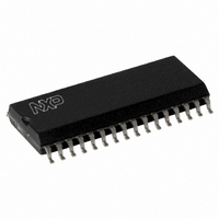
SLRC40001T/OFE,112 NXP Semiconductors, SLRC40001T/OFE,112 Datasheet - Page 10

SLRC40001T/OFE,112
Manufacturer Part Number
SLRC40001T/OFE,112
Description
IC I.CODE SLRC400 READER 32-SOIC
Manufacturer
NXP Semiconductors
Series
I-Coder
Datasheets
1.SLRC40001TOFE112.pdf
(130 pages)
2.SLRC40001TOFE112.pdf
(132 pages)
3.SLRC40001TOFE112.pdf
(101 pages)
Specifications of SLRC40001T/OFE,112
Rf Type
Read Only
Frequency
13.56MHz
Features
ISO15693, ISO18000-3
Package / Case
32-SOIC (0.300", 7.50mm Width)
Product
RFID Readers
Operating Temperature Range
- 25 C to + 85 C
Lead Free Status / RoHS Status
Lead free / RoHS Compliant
Lead Free Status / RoHS Status
Lead free / RoHS Compliant, Lead free / RoHS Compliant
Other names
568-1124-5
935269551112
SLRC400
SLRC41TOFED
935269551112
SLRC400
SLRC41TOFED
- Current page: 10 of 130
- Download datasheet (689Kb)
Philips Semiconductors
I•CODE Reader IC
3.2
Pin Types: I...Input;
1
refer to chapter 4.
These pins offer different functionality according to the selected µ-Processor interface type. For detailed information
PIN
10
11
20
21
22
12
13
23
24
25
26
…
1
2
3
4
5
6
7
8
9
1
1
1
1
1
Pin Description
OSCIN
IRQ
RFU
SIGOUT
TX1
TVDD
TX2
TVSS
NCS
NWR
R/NW
nWrite
NRD
NDS
nDStrb
DVSS
D0 to D7
AD0 to AD7
ALE
AS
nAStrb
A0
nWait
A1
A2
DVDD
AVDD
SYMBOL
TYPE
PWR
PWR
PWR
PWR
PWR
I/O
I/O
O...Output;
O
O
O
O
O
I
I
I
I
I
I
I
I
I
I
I
I
I
I
I
Crystal Oscillator Input: input to the inverting amplifier of the oscillator.
This pin is also the input for an externally generated clock (f
Interrupt Request: output to signal an interrupt event
This Pin should be connected to Ground
I•CODE
ISO 15693
Transmitter 1: delivers the modulated 13.56 MHz carrier frequenzy
Transmitter Power Supply: supplies the output stage of TX1 and TX2
Transmitter 2: delivers the modulated 13.56 MHz carrier frequenzy
Transmitter Ground: supplies the output stage of TX1 and TX2
Not Chip Select: selects and activates the µ-Processor interface of the SL RC400
Not Write: strobe to write data (applied on D0 to D7) into the SL RC400 register
Read Not Write: selects if a read or write cycle shall be performed.
Not Write: selects if a read or write cycle shall be performed
Not Read: strobe to read data from the SL RC400 register (applied on D0 to D7)
Not Data Strobe: strobe for the read and the write cycle
Not Data Strobe: strobe for the read and the write cycle
Digital Ground
8 Bit Bi-directional Data Bus
8 Bit Bi-directional Address and Data Bus
Address Latch Enable: strobe signal to latch AD0 to AD5 into the internal address
latch when HIGH.
Address Strobe: strobe signal to latch AD0 to AD5 into the internal address latch
when HIGH.
Not Address Strobe: strobe signal to latch AD0 to AD5 into the internal address latch
when LOW.
Address Line 1: Bit 0 of register address
Not Wait: signals with LOW that an access-cycle may started and with HIGH that it
may be finished.
Address Line 1: Bit 1 of register address
Address Line 2: Bit 2 of register address
Digital Power Supply
Analog Power Supply
Interface Output: delivers a serial data stream according to I•CODE1 and
PWR...Power
10
DESCRIPTION
Product Specification Rev. 3.1 August 2004
osc
= 13.56 MHz).
SL RC400
Related parts for SLRC40001T/OFE,112
Image
Part Number
Description
Manufacturer
Datasheet
Request
R
Part Number:
Description:
NXP Semiconductors designed the LPC2420/2460 microcontroller around a 16-bit/32-bitARM7TDMI-S CPU core with real-time debug interfaces that include both JTAG andembedded trace
Manufacturer:
NXP Semiconductors
Datasheet:

Part Number:
Description:
NXP Semiconductors designed the LPC2458 microcontroller around a 16-bit/32-bitARM7TDMI-S CPU core with real-time debug interfaces that include both JTAG andembedded trace
Manufacturer:
NXP Semiconductors
Datasheet:
Part Number:
Description:
NXP Semiconductors designed the LPC2468 microcontroller around a 16-bit/32-bitARM7TDMI-S CPU core with real-time debug interfaces that include both JTAG andembedded trace
Manufacturer:
NXP Semiconductors
Datasheet:
Part Number:
Description:
NXP Semiconductors designed the LPC2470 microcontroller, powered by theARM7TDMI-S core, to be a highly integrated microcontroller for a wide range ofapplications that require advanced communications and high quality graphic displays
Manufacturer:
NXP Semiconductors
Datasheet:
Part Number:
Description:
NXP Semiconductors designed the LPC2478 microcontroller, powered by theARM7TDMI-S core, to be a highly integrated microcontroller for a wide range ofapplications that require advanced communications and high quality graphic displays
Manufacturer:
NXP Semiconductors
Datasheet:
Part Number:
Description:
The Philips Semiconductors XA (eXtended Architecture) family of 16-bit single-chip microcontrollers is powerful enough to easily handle the requirements of high performance embedded applications, yet inexpensive enough to compete in the market for hi
Manufacturer:
NXP Semiconductors
Datasheet:
Part Number:
Description:
The XA-S3 device is a member of Philips Semiconductors? XA(eXtended Architecture) family of high performance 16-bitsingle-chip microcontrollers
Manufacturer:
NXP Semiconductors
Datasheet:

Part Number:
Description:
The NXP BlueStreak LH75401/LH75411 family consists of two low-cost 16/32-bit System-on-Chip (SoC) devices
Manufacturer:
NXP Semiconductors
Datasheet:

Part Number:
Description:
The NXP LPC3130/3131 combine an 180 MHz ARM926EJ-S CPU core, high-speed USB2
Manufacturer:
NXP Semiconductors
Datasheet:

Part Number:
Description:
The NXP LPC3141 combine a 270 MHz ARM926EJ-S CPU core, High-speed USB 2
Manufacturer:
NXP Semiconductors

Part Number:
Description:
The NXP LPC3143 combine a 270 MHz ARM926EJ-S CPU core, High-speed USB 2
Manufacturer:
NXP Semiconductors

Part Number:
Description:
The NXP LPC3152 combines an 180 MHz ARM926EJ-S CPU core, High-speed USB 2
Manufacturer:
NXP Semiconductors

Part Number:
Description:
The NXP LPC3154 combines an 180 MHz ARM926EJ-S CPU core, High-speed USB 2
Manufacturer:
NXP Semiconductors

Part Number:
Description:
Standard level N-channel enhancement mode Field-Effect Transistor (FET) in a plastic package using NXP High-Performance Automotive (HPA) TrenchMOS technology
Manufacturer:
NXP Semiconductors
Datasheet:


