M0516ZAN Nuvoton Technology Corporation of America, M0516ZAN Datasheet - Page 7
M0516ZAN
Manufacturer Part Number
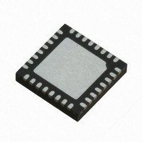
M0516ZAN
Description
IC MCU 32BIT 64KB FLASH 33QFN
Manufacturer
Nuvoton Technology Corporation of America
Series
NuMicro M051™r
Specifications of M0516ZAN
Core Processor
ARM Cortex-M0
Core Size
32-Bit
Speed
50MHz
Connectivity
EBI/EMI, I²C, IrDA, SPI, UART/USART
Peripherals
Brown-out Detect/Reset, LVD, POR, PWM, WDT
Number Of I /o
24
Program Memory Size
64KB (64K x 8)
Program Memory Type
FLASH
Ram Size
4K x 8
Voltage - Supply (vcc/vdd)
2.5 V ~ 5.5 V
Data Converters
A/D 5x12b
Oscillator Type
Internal
Operating Temperature
-40°C ~ 85°C
Package / Case
33-WFQFN Exposed Pad
Lead Free Status / RoHS Status
Lead free / RoHS Compliant
Eeprom Size
-
Available stocks
Company
Part Number
Manufacturer
Quantity
Price
Company:

Part Number:
M0516ZAN
Manufacturer:
Nuvoton
Quantity:
200
Part Number:
M0516ZAN
Manufacturer:
NUVOTON
Quantity:
20 000


™
NuMicro M051
Series Technical Reference Manual
Figure 6.5-15 GC Mode ............................................................................................................... 185
Figure 6.6-1 PWM Generator 0 Clock Source Control................................................................. 188
Figure 6.6-2 PWM Generator 0 Architecture Diagram................................................................. 189
Figure 6.6-3 PWM Generator 2 Clock Source Control................................................................. 190
Figure 6.6-4 PWM Generator 2 Architecture Diagram................................................................. 190
Figure 6.6-5 PWM Generator 4 Clock Source Control................................................................. 191
Figure 6.6-6 PWM Generator 4 Architecture Diagram................................................................. 191
Figure 6.6-7 PWM Generator 6 Clock Source Control................................................................. 192
Figure 6.6-8 PWM Generator 6 Architecture Diagram................................................................. 192
Figure 6.6-9 Legend of Internal Comparator Output of PWM-Timer ........................................... 193
Figure 6.6-10 PWM-Timer Operation Timing............................................................................... 194
Figure 6.6-11 PWM Double Buffering Illustration......................................................................... 194
Figure 6.6-12 PWM Controller Output Duty Ratio........................................................................ 195
Figure 6.6-13 Paired-PWM Output with Dead Zone Generation Operation ................................ 195
Figure 6.6-14 Capture Operation Timing ..................................................................................... 196
Figure 6.6-15 PWM Group A PWM-Timer Interrupt Architecture Diagram.................................. 197
Figure 6.6-16 PWM Group B PWM-Timer Interrupt Architecture Diagram.................................. 198
Figure 6.7-1 SPI Block Diagram................................................................................................... 232
Figure 6.7-2 SPI Master Mode Application Block Diagram.......................................................... 233
Figure 6.7-3 SPI Slave Mode Application Block Diagram............................................................ 233
Figure 6.7-4 Two Transactions in One Transfer (Burst Mode) .................................................... 235
Figure 6.7-5 Byte Reorder............................................................................................................ 236
Figure 6.7-6 Timing Waveform for Byte Suspend........................................................................ 237
Figure 6.7-7 Variable Serial Clock Frequency ............................................................................. 238
Figure 6.7-8 SPI Timing in Master Mode ..................................................................................... 239
Figure 6.7-9 SPI Timing in Master Mode (Alternate Phase of SPICLK) ...................................... 240
Figure 6.7-10 SPI Timing in Slave Mode ..................................................................................... 240
Figure 6.7-11 SPI Timing in Slave Mode (Alternate Phase of SPICLK) ...................................... 241
Figure 6.8-1 Timer Controller Block Diagram .............................................................................. 256
Figure 6.8-2 Clock Source of Timer Controller ............................................................................ 256
Figure 6.9-1 Timing of Interrupt and Reset Signal ....................................................................... 266
Figure 6.9-2 Watchdog Timer Clock Control................................................................................ 267
Publication Release Date: Sept 14, 2010
- 7 -
Revision V1.2
Related parts for M0516ZAN
Image
Part Number
Description
Manufacturer
Datasheet
Request
R

Part Number:
Description:
Manufacturer:
Nuvoton Technology Corporation of America
Datasheet:
Part Number:
Description:
Manufacturer:
Nuvoton Technology Corporation of America
Datasheet:
Part Number:
Description:
Manufacturer:
Nuvoton Technology Corporation of America
Datasheet:
Part Number:
Description:
Manufacturer:
Nuvoton Technology Corporation of America
Datasheet:
Part Number:
Description:
Manufacturer:
Nuvoton Technology Corporation of America
Datasheet:
Part Number:
Description:
Manufacturer:
Nuvoton Technology Corporation of America
Datasheet:
Part Number:
Description:
Manufacturer:
Nuvoton Technology Corporation of America
Datasheet: