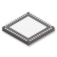
DS92LV2421SQE/NOPB National Semiconductor, DS92LV2421SQE/NOPB Datasheet - Page 35

DS92LV2421SQE/NOPB
Manufacturer Part Number
DS92LV2421SQE/NOPB
Description
IC SER/DESER 10-75MHZ 24B 48LLP
Manufacturer
National Semiconductor
Datasheet
1.DS92LV2421SQENOPB.pdf
(40 pages)
Specifications of DS92LV2421SQE/NOPB
Serdes Function
Serialiser
Ic Input Type
LVCMOS
Ic Output Type
CML
No. Of Inputs
1
No. Of Outputs
1
Supply Voltage Range
1.71V To 1.89V
Driver Case Style
LLP
No. Of Pins
48
Svhc
No SVHC
Rohs Compliant
Yes
Lead Free Status / RoHS Status
Lead free / RoHS Compliant
Other names
DS92LV2421SQE/NOPBTR
Available stocks
Company
Part Number
Manufacturer
Quantity
Price
Company:
Part Number:
DS92LV2421SQE/NOPB
Manufacturer:
NSC
Quantity:
1 250
Part Number:
DS92LV2421SQE/NOPB
Manufacturer:
TI/德州仪器
Quantity:
20 000
Applications Information
DISPLAY APPLICATION
The DS92LV2421/DS92LV2422 chipset is intended for inter-
face between a host (graphics processor) and a Display. It
supports an 24-bit color depth (RGB888). In a RGB888 ap-
plication, 24 color bits (D[23:0), Pixel Clock (CLKIN) and three
control bits (C1, C2, C3) are supported across the serial link
with CLK rates from 10 to 75 MHz. The chipset may also be
used in 18-bit color applications. In this application three to
six general purpose signals may also be sent from host to
display.
The Des is expected to be located close to its target device.
The interconnect between the Des and the target device is
typically in the 1 to 3 inch separation range. The input capac-
itance of the target device is expected to be in the 5 to 10 pF
range. Care should be taken on the CLK output trace as this
signal is edge sensitive and strobes the data. It is also as-
sumed that the fanout of the Des is one. If additional loads
need to be driven, a logic buffer or mux device is recom-
mended.
FIGURE 32. DS92LV2421 Typical Connection Diagram — Pin Control
35
TYPICAL APPLICATION CONNECTION
Figure 32
in Pin control mode for 24-bit Application. The LVDS outputs
require 100 nF AC coupling capacitors to the line. The line
driver includes internal termination. Bypass capacitors are
placed near the power supply pins. At a minimum, four 0.1 µF
capacitors and a 4.7 µF capacitor should be used for local
device bypassing. System GPO (General Purpose Output)
signals control the PDB and BISTEN pins. In this application
the RFB pin is tied Low to latch data on the falling edge of the
CLKIN. In this example the cable is long, therefore the VOD-
SEL pin is tied High and a De-Emphasis value is selected by
the resistor R1. The interface to the host is with 1.8 V LVC-
MOS levels, thus the VDDIO pin is connected also to the 1.8V
rail. The optional Serial Bus control is not used in this exam-
ple, thus the SCL, SDA and ID[x] pins are left open. A delay
cap is placed on the PDB signal to delay the enabling of the
device until power is stable.
shows a typical application of the DS92LV2421 Ser
30110144
www.national.com


